This thread has been locked.

If you have a related question, please click the "Ask a related question" button in the top right corner. The newly created question will be automatically linked to this question.

ADS8331: Issue with ADS8331

Part Number: ADS8331
Other Parts Discussed in Thread: OPA320

Hi ,

I am Rahul from WT microelectronics.

One of my customer using  ADC8331 and communicate with MCU through SPI.

Issue is that data received by ADC is not correct.

Please check below

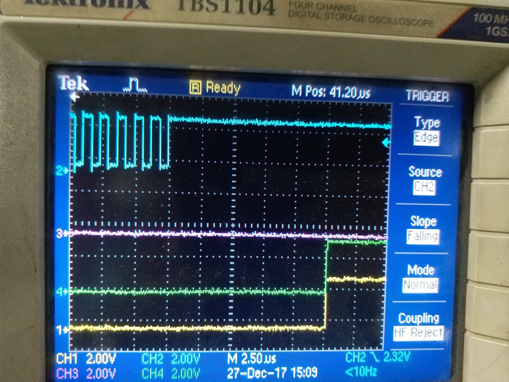
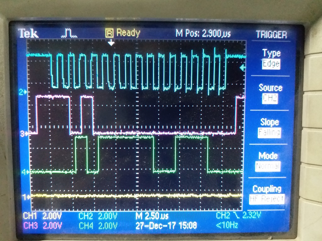
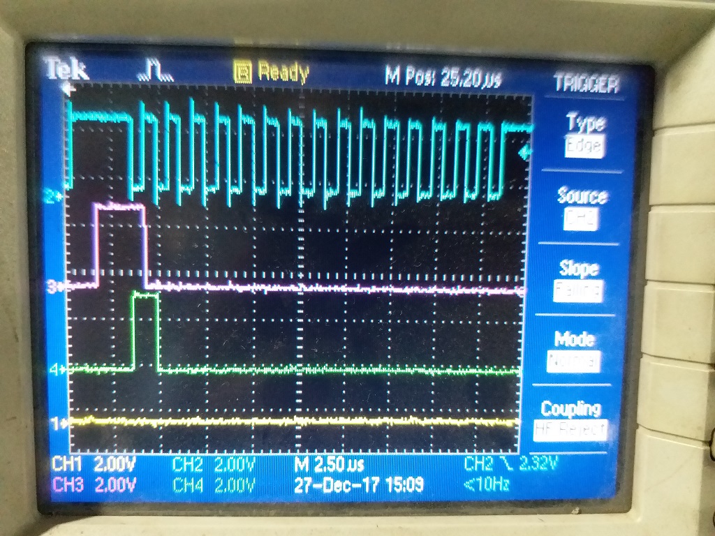
Data received.= 0X17CE(6094) 

TAG BITS= 0b0100000000000000


but pin voltage is 2.462V @ channel no. 2.


Vref = 4.105V

CFR= 110011111111


packet to read data = 0b1101000000000000

Dummy to receive tag bits = 0b1000000000000000
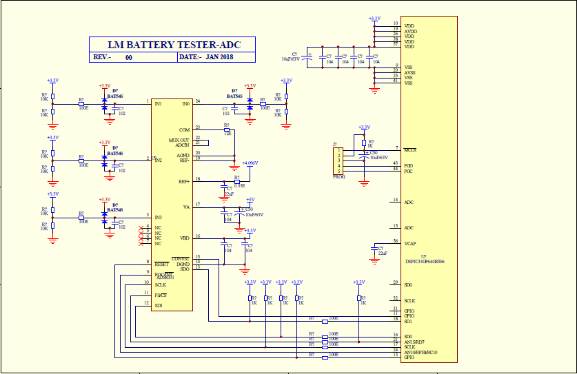
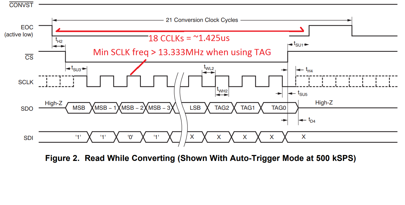
 

 in images

blue is clock

yellow is Chip select

green is SDO(MISO)

pink is SDI (MOSI).

Please help to solve this issue.

thanks

Rahul

WT microelectronics

rahul@wtmec.com

9540488549

  • HI Rahul,

    Please post an schematic showing the ADS8331 device interface connections: CS, SCLK, SDI, SDO, CONVST, EOC, RESET.   Please also show the VA and VBD supply connections, supply bypass capacitors, reference drive circuit with bypass capacitors and  the driver amplifiers.

    The post above mentions images showing interface signals; however, the images do not appear to be included in the post.

    Please also include a couple of oscilloscope plots of the interface signals during a read transaction.   Please include  CS, SCLK, SDI, SDO, CONVST, EOC on the oscilloscope plot so we can verify the timing.   Please place the oscilloscope probes right at the pins of the ADS8831.

    Many Thanks,

    Best Regards,

    Luis

  • Hi Luis,

    Please check attach schematic and waveforms.

    RH BATTERY BETTERY TESTER ADC (1).pdf

    Thanks

    Regards

    Rahul

  • Hi Rahul,

    Thank you for the oscilloscope plots. The CFR register is set to 1100 1111 1111: the device is set to auto channel select mode, auto-trigger mode, sampling rate of 500kSPS, and using internal oscillator for conversion clock.

    The ADC conversion data read operation can be performed while the ADC is converting, or alternatively, the data may be read while the device is sampling, as shown on Figure1 and Figure 2 of the datasheet.

    For example, Figure 2 of the datasheet shows the timing required when performing “Read While Converting with Auto Trigger mode at 500kSPS”, where the data read frame must be completed while the EOC indicator is low. The conversion time is x18 int oscillator clocks, or assuming max internal oscillator frequency of 12.6MHz, the minimum conversion time is approximately ~1,425us.

    Per Table 7 (p35), in order to read the 16-bit conversion data and the 3 TAG bits, you require at least 19 SPI SCLKs.   Therefore, in order to complete the data read operation while converting the minimum required SCLK frequency is >~13.33 MHz or a SCLK frequency faster than 13.5MHz.

    -The oscilloscope suggests that you are using an SCLK frequency of 800kHz. Is this correct?  Please note, if you are planning to use full-throughput of 500kSPS with tag mode, you will require a SCLK frequency above 14MHz.

    - The schematic shows you are using a voltage divider with 10kOhm resistors, and RC filter with 100ohms and 1nF capacitor. Please note that the ADS8331 is a SAR ADC, and the device needs to be driven with a very low impedance source when used a max throughput.  The driver amplifier circuit needs to be able to completely re-charge the internal sample and hold capacitor and settle within 1 LSB (least significant bit) during the acquisition period .

    The voltage divider in the schematic is not able to drive the ADS8331 at 500kSPS. If you are required to use the ADS8331 at full throughput of 500kSPS, buffer amplifiers at the inputs of the mux are required to drive the ADS8331. Alternatively, you could consider using the manual-trigger mode and slow down the sampling rate considerably, to a much slower sampling rate in the order of ~20KSPS.   The applications section of the datasheet shows an optimal input driver circuit using the OPA320 on Figure 53 (p41), and an optimal reference driver supporting full throughput of 500kSPS.

    - Please let me know the max sampling rate required on this application.

    Thank you ,

    Regards,

    Luis

  • Hi Rahul,

    I have not heard back from you regarding the sampling rate requirements for this the application and/or if you were able to get valid conversion results after slowing the data rate or after modifying the design with the input driver circuit. I will close this post, but if you have additional queries, please post back with details.

    Thank you,

    Luis