This thread has been locked.

If you have a related question, please click the "Ask a related question" button in the top right corner. The newly created question will be automatically linked to this question.

ADS1015: Abou AIN+ pin voltage drop

Part Number: ADS1015
Other Parts Discussed in Thread: ADS1000, ADS1115, ADS1120

Hi,

Could you tell me about ADS1015 AIN+ pin?
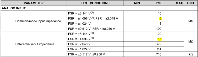
Customer is considering ADS1015 with the following figure configuration.

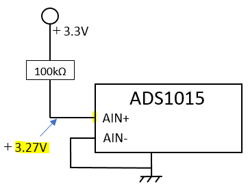
The results measured by the tester, the AIN+ pin was 3.27V.
Could you give me your opinion on the reason to drop the 30mV ?
Customers want to grasp error factors in order to accurately measure voltages.

Best Regards,
Yusuke/Japan Disty


  • Tsukui-san,


    The drop in voltage (~0.03V) is due to the input impedance. The ADC samples the input voltage with sampling capacitors at a modulator frequency of 250kHz. This is described in the datasheet on pages 9 and 10. Table 2 shows the differential input impedance, which varies with the full scale input range in the datasheet on page 10.

    On top of the differential input impedance, there is a common-mode impedance that also varies with the full scale input range. Specifications are listed in the Electrical Characteristics on page 3 of the datasheet. The equvalent input impedances are shown in Figure 12.

    If they are using a range of ±4.096V, the differential input impedance is 15MΩ and the common mode impedance is 6MΩ. In parallel, these become 4.3MΩ. If the supply is 3.3V, and the series input resistance is 100kΩ then you can expect the input to be voltage divided to:

    3.3V * 4.3MΩ / (100kΩ + 4.3MΩ) = 3.23V

    If the range is ±6.144V, the input would be near 3.25V.


    Joseph Wu

  • Joseph-san,

    Thank you for your kind support.
    I understood your explanation.
    Let me ask you one more thing.

    The calculated value and the measured value are different.
    I think that this cause is due to the dispersion of the resistor value.

    1.Do you have information on the Min and Max values of resistor value?


    2.If there is no resistor variation information,
       Could you tell me how to suppress variation?
       Customers want to minimize voltage drop variations as much as possible.

    Best Regards,
    Yusuke/Japan Disty

  • Tsukui-san,


    There are a few things that may affect the measurement of this value. First, the multimeter probably has an input impedance that is similar to the input impedance of the device. The measured value may be different than the actual value just because of the input impedance of the multimeter.

    Second, there may also be leakage currents from the input pins because of the ESD structures. These reverse bias diodes may cause some input current which will change over temperature. This is likely to be less than 1nA at room temperature, but the input current may increase at higher temperatures.

    Based on the differential and common-mode input impedance mechanism, I'm not sure what the variation of the input impedance will be. It is dependent on the input capacitance variation, and the sampling time variation. It is likely that the variation is rather high.

    Regardless, the best way to minimize the voltage drop is to reduce the series input impedance. I recommend that the series input impedance is less than 10kΩ.


    Joseph Wu
  • Joseph-san,

    Thank you for your quick and polite response. 
    I will report your information to customers.

    Let me ask you one more thing.
    Could you tell me how to voltage minimize variations.
    For example, method of calibrating every device etc.
    Customers want to suppress voltage fluctuations.

    And Incidentally,
    Is there information on the common-mode impedance min max and Differential impedance min max?
    For example, Do you have information such as lot sampling data?

    Best Regards,
    Yusuke/Japan Disty

  • Tsukui-san,


    On some of our 24-bit devices, we may test the input current/input impedance of the ADC, but on the ADS1000 we do not. I'm sorry but we don't have any final test data or lot sampling data for this parameter and we don't provide a minimum or maximum.


    Joseph Wu
  • Joseph-san,

    Thank you for your information.
    I understood the situation.

    Let me ask you one more thing.
    Could you tell me how to voltage minimize variations?
    For example, method of calibrating every device etc.
    Customers want to suppress voltage fluctuations.

    Could you give me your advice?

    Best Regards,
    Yusuke/Japan Disty
  • Tsukui-san,


    I don't have a good way to minimize the voltage variations. The input current will vary depending on several factors as I've mentioned. There are only a few things I can think of to lower this voltage:

    1. Reduce the series resistance at the input of the device.

    2. Use a higher input range so that the equivalent differential and common-mode impedance are higher. To keep the same resolution, the customer could use the ADS1115 instead.

    3. Use a different device with a lower input current. The ADS1120 may be an option. It likely has more features than necessary for the application, but does have a lower input current. Note that it uses an SPI interface.


    Joseph Wu