This thread has been locked.

If you have a related question, please click the "Ask a related question" button in the top right corner. The newly created question will be automatically linked to this question.

LM15851: clocking LM15851

Part Number: LM15851
Other Parts Discussed in Thread: LMK04610, LMX2572, LMK04828, LMX2594, TRF3765, LMX2582

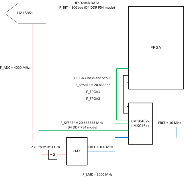
Hi! I need to feed LM15851 with 4GHz device clock + SYSREF and an FPGA with some other device clock + SYSREF (a JESD204B system). As I have seen, there is no suitable clocking solution integrated into a single IC with so high output frequency and JESD204B support. So, it seems that LMK04610 and LMX2572 cascaded somehow would be suitable. Would you be so kind to give some explanation on clocking architecture using these devices? How should the two clocking devices be connected together and with LM15851 and FPGA? What would be SYSREF signal architecture?
Maybe there are more suitable devices, but these two were chosen due to their low power consumption. Maybe you can recommend other devices. Thanks in advance.

  • Hello Vic,
    I have sent your question to an engineer familiar with the LM15851
    Regards,
    Brian
  • Ok, thanks, Brian.

  • By the way. The only forum that I could chose is the Medical Forum. Can you help me please and move this thread to the High Speed Data Converters Forum? Thanks.
  • Vic, don't worry you are in the right forum and I have the right guy looking at this.
    Regards,
    Brian
  • Hi Vic

    The basic concept of what you need to accomplish is shown in the figure below. The LMK048xx device is needed to create the FPGA clocks and SYSREF for FPGA. It can also create the ADC SYSREF if that signal is needed. The LM15851 can operate without SYSREF, however in this case neither deterministic system latency, or multi-device synchronization can be achieved.

    The LMX2572 is a viable choice for the 4 GHz ADC clock source.The LMK04xxx outputs must be synchronous to the ADC clock signal. There are a number of ways to do this, and the best one depends on the needed ADC clock frequency and the VCO capabilities of the selected LMK04xxx device. For a 4 GHz ADC clock, the LMK04610 can be configured for operation at 6 GHz. This clock can be divided down to create the needed reference clock for the LMX2572 as well as the FPGA clocks and SYSREF.

    If the LMK VCOs cannot provide a good frequency related to the needed ADC clock then the architecture show below can be used, since it uses the LMK device in clock distribution mode.

    The LM15851EVM uses the LMK04828 in distribution mode, and also utilizes PLL1 to synchronize a 100 MHz VCXO to an optional 10 MHz external reference. This enables synchronization of the data converter to other system devices.The LM15851EVM uses the TRF3765 PLL/VCO device for the 4 GHz clock, but the following devices released since the board was designed would be better choices: LMX2572, LMX2594, LMX2582

    The LM15851EVM schematics are available here: /cfs-file/__key/communityserver-discussions-components-files/73/7750.ADC12JXXXXEVM_5F00_A01_5F00_Schematic-Prints.PDF

    Best regards,

    Jim B

  • Thanks a lot, Jim. I'll consider the two architectures you proposed. Can you help me with a few more questions? As I understood, in the JESD204B standard the device clocks at the inputs of linked devices must be phase aligned. Some of the clocks may be multiples of the other, but in certain moments rising edges of the device clocks must coincide. The SYSREF signals are used to identify the rising edges of the device clocks to which local frame and multiframe clocks in all devices in a JESD link must be rising-edge aligned. These are exactly the same moments through the all JESD link. So in a JESD system all the clocks are phase alligned. Am I right? So can you give some comments on phase relationships between LMK and LMX outputs in the first figure. As I understood, the SYSREF signal is generated in the LMK and propagates through the LMX which is in the SYSREF Repeater Mode. The 4 GHz clock output of the LMX and the SYSREF output are in needed phase relationships with each other. This phase relationships can be adjusted by SYSREF delay circuitry of the LMX. Am I right? Is it assumed that the LMX outputs which clock the ADC are phase related to the LMK outputs which clock the FPGA?
  • Hi Vic

    In general, the following clocking requirements apply to JESD204B Subclass 1 links where deterministic latency is desired.

    1. The TX and RX devices in a link must each receive a SYSREF signal with constant phase relationship. Phase offset is OK as long as it is relatively constant.
    2. The TX and RX devices must each receive a Device Clock. These clocks may be different frequencies, but must have an integer frequency ratio and relatively constant phase offset.
    3. At each device, SYSREF must be consistently capture on the same edge of Device Clock. Setup/Hold timing may need to be adjusted at either the clock generator or at the TX or RX device to ensure this is the case.

    If all 3 of these requirements are met, then the devices in the system will have internal LMFC (local multi-frame clock) timing with constant phase relationshps, which will support deterministic latency.

    If you need deterministic latency in your system, then the ADC Device Clock to SYSREF timing is the most stringent requirement to meet. You are correct that the LMX2572 SYSREF repeater feature can be used to ensure constant phase alignment between DEVCLK and SYSREF to the ADC. If 2 LMK outputs are used for the LMX2572 reference and SYSREF inputs, then the relative phase of those signals should be relatively well controlled. The LMKxxxx datasheet will have more information regarding skew of the outputs.

    The LMX2572 SYSREF delay feature can be used if needed to optimize the relative timing of the 2 outputs. The ADC also has adjustable delay on the SYSREF path, and timing verification features that should be used to ensure setup and hold timing is adequate.

    Some systems with multiple ADCs or DACs may require more stringent timing requirements if there is a need for phase aligned ADC input sampling or DAC updating. In these systems the ADC and DAC device clocks may need to be fine tuned to achieve the required sample alignment. If these clocks are fine tuned then the relative timing between SYSREF and Device Clock may need some re-adjustment to ensure setup and hold times are still met.

    If deterministic latency is not required, then some of the devices may not require SYSREF. The LM15851 is one of these devices. The internal LMFC will be self generated even if SYSREF is not applied. However the LMFC inside the LM15851 will have a random phase relationship to SYSREF and the LMFC inside the FPGA data receiver. If this is the case for your system you just need to ensure the FPGA Device Clock and SYSREF timing have adequate setup and hold, and won't need to use the LMX2572 SYSREF repeater function.

    I hope this is helpful.

    Best regards,

    Jim B

  • Hi, Jim. Thanks a lot for the fast and detailed responses. This information is very helpful for me. Best regards, Vic.