This thread has been locked.

If you have a related question, please click the "Ask a related question" button in the top right corner. The newly created question will be automatically linked to this question.

DAC7811: DAC7811 Bandwidth across attenuation

Part Number: DAC7811
Other Parts Discussed in Thread: DAC8811, DAC8822, DAC8820

Hi, Experts:

May I have a question of the reference multiplying bandwidth for the multiplying DAC DAC7811.

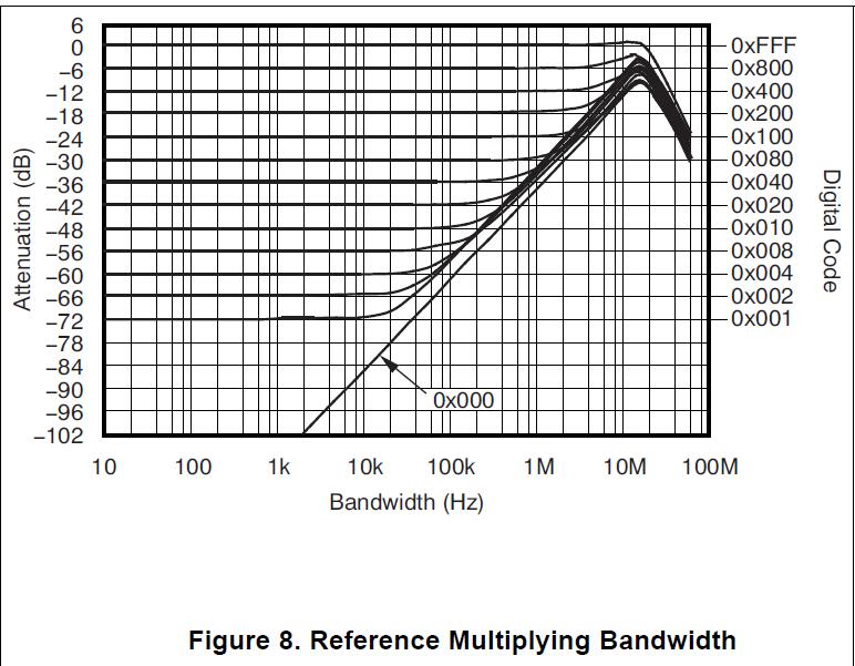
As the digital codes goes smaller, the current going out from Iout1 will be smaller, namely the impedance looking into Iout1 pin will be larger, then the attenuation is larger. 

For the opertion amplifier, if the Rgain goes larger, the Noise Gain will be 1 +Rf/Rg which will goes smaller. Hence the BW will come larger when attenuation increases. My understanding looks wrong compared to our plot. 

Could you kindly please help me to understand the theroy behind this? Thank you.

Yarn

  • Hi Yarn,

    Thank you for your query. The multiplying bandwidth of an MDAC is not defined by the output opamp. The opamp is usually chosen to have a larger bandwidth than the MDAC. What is shown in Fig 8 of the datasheet is mainly the characteristic of the MDAC. The gain-bandwidth analysis you have done will apply to the opamp, not the MDAC.

    Hope I have answered your question.

    Regards,
    Uttam Sahu
    Applications Engineer, Precision DACs
  • Hi, Sahu:

    Thanks a lot for your prompt help.

    Would you please help to explain a little bit why the bandwidth of the MDAC will decrease as the attenuation increases? That will help me underatand better. Thanks!

    Yarn
  • Hi Yarn,

    I am discussing to the internal team in order to get a proper explanation for this. I will get back by tomorrow.

    Regards,
    Uttam
  • Hi Yarn,

    I got a nice answer from the design team and I don't want to distort it by rephrasing in my words. So, I am putting it here as is:

    "The reason for the bandwidth decreasing vs. code is because as lower code settings are activated, the signal path from the reference to the switched bit has increasing impedance.  With the mostly fixed capacitance at the IOUT terminal, this limits the bandwidth.  If you look at the DAC8811 pds simplified R2R ladder figure on page 8, you will see the reference comes in at the left side of the schematic and is applied equally across all MSB segments.  However, to bit 4 it goes through an additional R leg.  To bit 5 it will have an additional R leg.  And so forth.  Also, the capacitances at the various R2R ladder node connections will cause a multi-stage filter action.  But hope this somewhat simplified explanation helps to understand this."

    There are Tina models for DAC8820 and DAC8822. You can check this behavior yourself. I have done a simplistic simulation with an opamp and it shows a similar behavior.

    Hope it clarifies your doubt.

    Regards,

    Uttam

  • Hi, Uttam:

    Thanks a lot for your kind explanation. Appreciate!

    Yarn