This thread has been locked.

If you have a related question, please click the "Ask a related question" button in the top right corner. The newly created question will be automatically linked to this question.

ADS1018-Q1: TUE calculation for FSR = +- 6.144V

Part Number: ADS1018-Q1
Other Parts Discussed in Thread: ADS1018, ADS1605

hi team

Customer would like to calculate TUE for ADS1018-Q1,

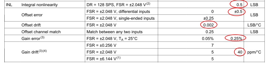
but D/S has only information for FSR = +- 2.048V as below.

the following TUE calculated is OK for FSR = +- 6.144V case ?

FSR = ±6.144V,

Resolution = FSR x 2 / 2^bits = 6.144V x 2 / 2^12 = 3[mV]

Max Offset =0.5[LSB],

Max Offset drift over temperature = 0.002 [LSB/⁰C] x (125⁰C - 25⁰C) = 0.2[LSB]

MAX INL = 0.5[LSB],

Max DNL = 0[LSB],

Max GainError = 0.25[%]/100 x FSR x 2 / Resolution = 0.25[%]/100 x 6.144V x 2 / 3[mV] = 10.24[LSB]

Max Gain Drift over temperature = 40[PPM/⁰C]/10000 x (125⁰C - 25⁰C) x FSR x 2 /Resolution = 40[PPM/⁰C]/10000 x (125⁰C - 25⁰C)/100  x 6.144V x 2 / 3[mV] = 16.384[LSB]

hence, Max TUE = SQRT[ Vos^2 + INL^2 + DNL^2 + GainError^2 ] = SQRT[(0.5+0.2)^2 + 0.5^2 + 0^2 + (10.24+16.384)^2] = ±26.637[LSB]

            Max TUE = 3[mV] x 26.637[LSB] =  ±79.91[mV]


  • Paul,


    There have be a couple of questions on the TUE of some of our devices lately. The method you show for TUE is close to what I think it should be but I think there should be a few corrections. I'll go through your values, and explain what I mean.

    The offset value of 0.5 LSB is still good (even if it is probably smaller than that). Also, the offset drift is 0.002 LSB/°C as a typical value. If you wanted a maximum value I would have taken the typical value and multiplied by 3x as a guess for the maximum. This would be 0.006 LSB/°C. If your temperature drifts from 25°C to 125°C then the drift would be about 0.6LSB.

    The INL on this device is very small, and is low sub-LSB for a value. Using 0.5 LSB is also ok but it is also likely much smaller than that. Regardless, it is also a small contribution to the TUE.

    The remaining gain error and gain error drift have the largest contribution to the TUE, as it is in your analysis. As you have, I would continue to use the max numbers as listed for the ±2.048V range. However, even if the input range setting is ±6.144V, the largest input signal that you can measure with the device is limited between GND and VDD. If the supply is +5V, the usable range of the device is ±5V. That would mean that the max gain error of ±0.25% is limited to ±4.16 Bits. This would be the number you use in your root sum of squares calculation.

    For the gain error drift, the 40ppm/°C number becomes 0.4% with a change of 100°C (assuming the worst case change from 25°C to 125°C). Again, with a 5V supply, the max gain error drift is ±0.4% translates to a gain error of ±6.67 bits.

    After that you can calculate the TUE from:

    TUE = SQRT ((0.5+0.6)^2 + (0.5)^2 + (4.16+6.67)^2) = 10.9 bits or about 32.7mV

    Again the gain error and gain error drift have the largest contribution for the TUE. The offset and INL have almost no contribution to this error.

    In case you hadn't seen it, a sample TUE calculation is outlined in the following application note:

    www.ti.com/.../slaa587.pdf

    Now, a colleague wrote something about calculating the TUE today. I would read it here:

    e2e.ti.com/.../688554

    The point is that TUE can be calculated with max values or typical values and they are often dominated by the gain error (as shown in the calculation). I'd note that the error from gain error is largest when the input is at full scale and smallest when the input is 0. Also, gain error may be calibrated depending on the operating conditions and limited if the temperature range is controlled.

    Regardless, the error you get from TUE calculations may be misleading, but I hope this helps explain it.


    Joseph Wu
  • Hi Joseph

    I understood your point,

    but I would like to point out the Gain Error Related calculated.

    ADS1018-Q1 can do Differentila and Single ended ADC.

    Gain Error depends on the usable imput range among FSR.

    So, the below are correct for FSR = +- 6.144V and VDD = 5V configuration ?

    [1] Differential case ==> the usable input will be - 5V ~ 5V.

        Max GainError = 0.25[%]/100 x Usable Input / Resolution = 0.25[%]/100 x (5V x 2) / 3[mV] = 8.34[LSB]

        Max Gain Drift over temperature = 40[PPM/⁰C]/10000 x (125⁰C - 25⁰C) x Usable Input / Resolution

                                                            = 40[PPM/⁰C]/10000 x (125⁰C - 25⁰C)/100  x (5V x 2) / 3[mV] = 13.34[LSB]

     [2] Single Ended case ==> the usable input will be 0V ~ 5V.

        Max GainError = 0.25[%]/100 x Usable Input / Resolution = 0.25[%]/100 x 5V / 3[mV] = 4.17[LSB]

        Max Gain Drift over temperature = 40[PPM/⁰C]/10000 x (125⁰C - 25⁰C) x Usable Input / Resolution

                                                            = 40[PPM/⁰C]/10000 x (125⁰C - 25⁰C)/100  x 5V / 3[mV] = 6.67[LSB]

  • Paul,


    The gain error is dependent only on the magnitude of the input signal and not on the range of the signal. As an example, let's say the gain error is 0.1% and there is not offset error. If the input is 5V, then the gain error is 5mV. If the input is 1V, then the gain error is 1mV. If the input is 0V, then the gain error is 0V. This value does not change with the range, it only changes with the magnitude of the input voltage.

    Going back to the ADS1018, the max gain error is ±0.25%. For a 5V input signal, this means that the gain error will be ±12.5mV. For a -5V input signal, it is the same. It does not make the gain error 25mV.

    I think my original calculation is correct. The numbers should be the same as the numbers you show for the single-ended case.


    Joseph Wu
  • Hi Joseph

    I got your meaning.

    previously I asked TUE for ADS1605 witch is Differential ADC,

    and BU replied that my calculation was OK to use FSR for calculating Max Gain and Offset even.

    that make me confused on whether I has to use FSR or the magnitude of the input signal for Offset and Gain.

    could you look at the below E2E blog and get your though to me ?


    e2e.ti.com/.../2257206

  • Paul,


    For the ADS1605, the offset is described as a percentage of the FSR, so your interpretation is correct. You would use the percentage of the full-scale range, which most of the time would be 2x the reference voltage (in the ADS1605 this is 2x1.467VREF). Note that the offset error is described as LSB in the ADS1018.

    However, the gain error is a percentage error from a full-scale input. It is not described as a percentage error from the full-scale range. The full-scale input is the largest input signal that you can put into the device for a measurement. For a differential input ADC, this would be half of the full-scale range (For the ADS1605, this would be 1.467xVREF).

    If you have a gain error of +0.25% and the differential input is ±5V. You can think of this as a +12.5mV error on +5V. Or you can think of this as a +12.5mV error on +5V also with a -12.5mV error on -5V. The percentage error is the same.


    Joseph Wu