This thread has been locked.

If you have a related question, please click the "Ask a related question" button in the top right corner. The newly created question will be automatically linked to this question.

DAC34H84: control signals for dac34h84 ?

Part Number: DAC34H84
Other Parts Discussed in Thread: DAC34SH84

Hello 

I am working on dac34h84 evm , i have some question ?

1. can i configure the DAC in fifo disabled mode ? if yes , then what will be reading frequency , reading frequency is depend upon what ?

2. can i give same frequency for data_clk and dac_clk , in fifo disable mode?

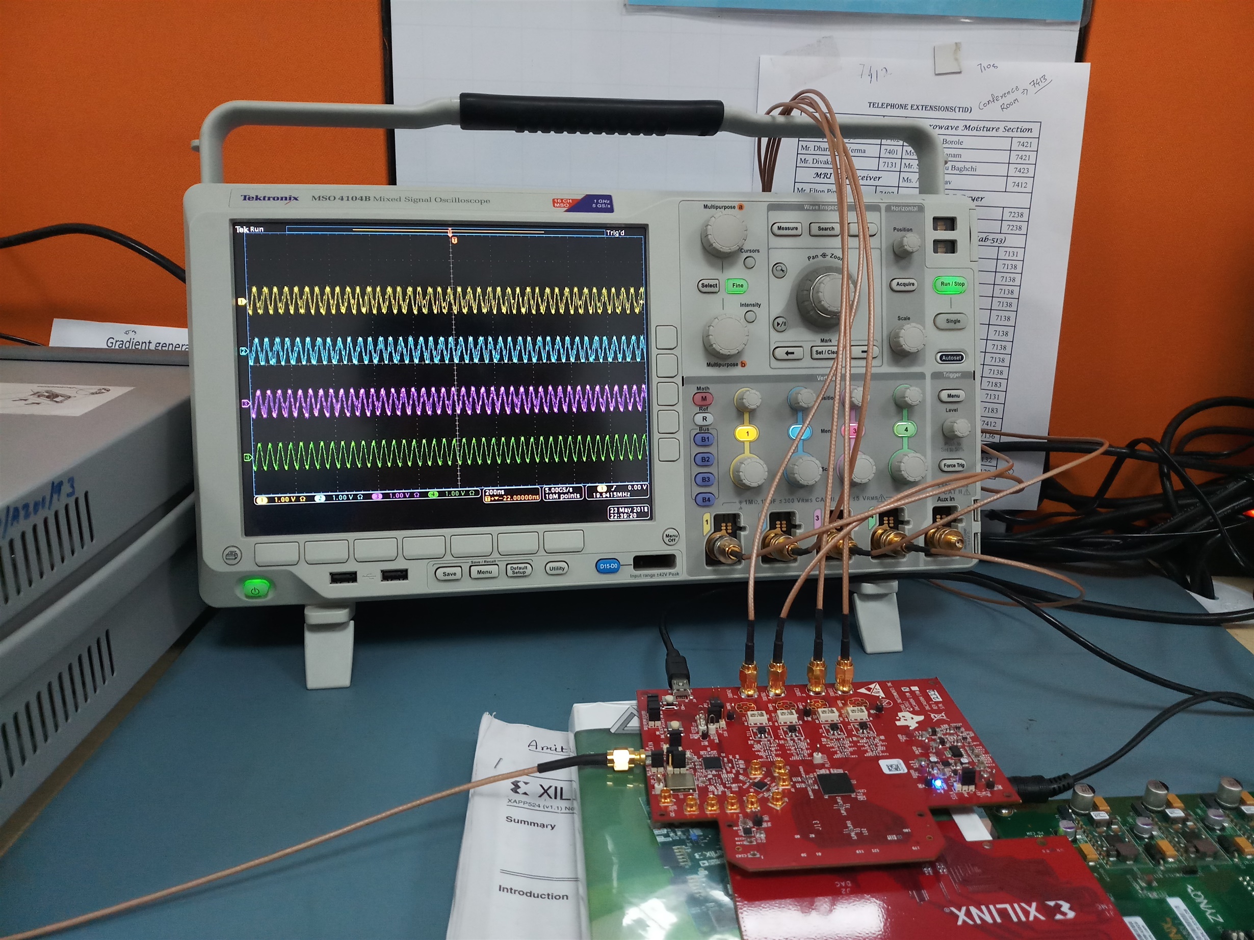
3. On dac34h84 evm "SH3" provides dacclk2 , can i provide this clk to the fpga or get it from fpga as i have fmc dac adapter ? as shown in the images below


4. If i generate the same pattern of wave as shown on the data sheet of dac34h84 page no 26, what are the extra signals which i need to take care like OSTR as i am not using fifo ? 

  • Hi Amit,

    1. TI does not recommend the usage of FIFO bypass mode. The reason is that with FIFO bypassed you have to ensure the DATACLK and DACCLK are absolutely synchronous without the possibility of shifting delay over time. 

    see app note below for reason to use FIFO

    2. It is possible with 1x interpolation filter since DATACLK and DACCLK rate would match.

    3. FPGA clock has high amount of jitter and will reduce the DAC performance significantly. If performance is not a concern, it may be possible.

  • thanks for reply @ kang,

    if I write data to fifo with data_clk frequency of 100Mhz what should be my dac_clk frequency ?
    and do i need to give OSTR signal also or it is optional ?
  • Hi Amit,

    The DACCLK depends on the interpolation ratio. For the DAC34H84 due to the data interface, you can simply multiply the dataclk * interpolation to get the DACCLK rate. We also have internal PLL to generate the DACCLK if it is too high frequency externally.

    OSTR is optional. You can refer to the app note posted before for options on syncing the FIFO.
  • @kang hisa , thanks for reply .sorry for replying late.


    I wrote code in VHDL which give sine wave of 10Mhz as input to the all the channel A, B, C and D with rising edge of the sync pin at the start of data transmission and my data clk is exact 90degree of the data sample. dataclk is 200Mhz,dac clk is 400Mhz given externally with interpolation of 2.
    when I program my FPGA no output comes on CRO but when I press reset on evm board it shows some output but not which I want.how i can reset dac with the gui software,there is usb reset button but i didn't find the dac self reset button on GUI software ?

    I am not using Pll, what should be my configuration on the evm software, that it must show some output after programming FPGA ?
  • Hi Amit,

    there are some example programming configuration files that you can adjust to fit your need. Please try them out and note the adjustments that you have made. I can help you review this.

    The FPGA clock requirement will depend on your RTL design. You will have to decide what clock to use to the entire FPGA design.

    -Kang
  • Hi Kang, 

    I tried the example configuration file "DAC34SH84_FDAC_1474p56MHz_4xint_NCOoff_QMCoff.txt" . 

    The procedure which did:

    1. I programmed my FPGA Xilinx zc702, then no output came on CRO,

    2. I pressed the reset button on the DAC evm 34h84 board, it starts showing some distorted output on CRO after that, I load the configuration file "DAC34SH84_FDAC_1474p56MHz_4xint_NCOoff_QMCoff.txt" .

    3.And changed the interpolation factor to 2. then we got the correct output of sine wave 20 MHZ. which we had generated using DDS in FPGA board. data_clk is 250 Mhz, DAc_clk is 500MHz.

    My question is when I again load the program from FPGA board, it shows nothing on CRO, I need to do the whole procedure again, give me suggestions on that.

  • @ kang
    i changed the fifo input setting, fifo output sync and fifo sync select to "sync" , which solved my issue.