This thread has been locked.

If you have a related question, please click the "Ask a related question" button in the top right corner. The newly created question will be automatically linked to this question.

16bit version of AD5443 with SPI I/F

Other Parts Discussed in Thread: DAC7811, DAC7822, DAC8820, DAC7821

Hi all, 

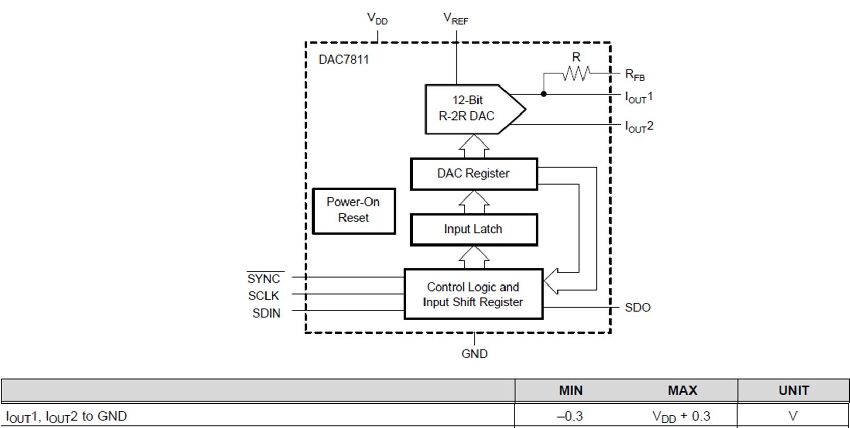
I am looking for 16-bit version DAC which performance is like DAC8821 and which function is similar to AD5443 (12-bit multiplying DAC).
And I plan to use it like below circuit.
There is about 2V differences between Iout2 and Digital GND.

Could you tell me the recommended DAC? 
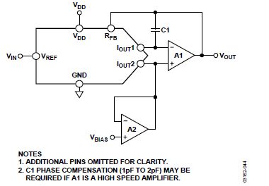
Regards,
Toshi

  • Toshi,

    DACs with this particular topology of a split IOUT1 and IOUT2 pin are somewhat unique / rare, and not just within TI. Some time ago we produced a reference design which discusses this approach along with it's limitations (www.ti.com/.../TIPD157), it should be noted that there are actually more limitations to this structure than the device datasheets may lead you to believe - I think this is because the designers at the time didn't really envision this use case. There are both functional and parametric implications to be aware of.

    The reference design points out all of the TI DACs that feature this architecture which include DAC7811, DAC7821, DAC7822, and DAC8820. DAC8820 is the only one which is a 16-bit device, but the interface is also a parallel bus which your application may or may not be able to accommodate.

    Can you elaborate on your requirements and why this approach is preferred? A simpler option may just be using a buffered voltage output DAC along with a single external amplifier to apply this offset, this would also have the benefit of using more conventionally available components.
  • Hello Duke-san,

    Sorry for interrupt you.

    But I would like you to confirm about below.

    >The reference design points out all of the TI DACs that feature this architecture which include DAC7811, DAC7821, DAC7822, and DAC8820.

    Actually, DAC8820 separate DGND and AGND, however, I guess that this is not same spec as DAC78xx.

    Here is block diagram of DAC7811.

    According to this, TI define spec "Iout 1 to GND" and "Iout 2 to GND".

    However, in case of DAC8820,

    TI define "Iout to GND" but not define "AGND to DGND".

    So I understood that user can separate GND, however not to insert bias voltage to AGND.

    So, could you please re-confirm user can apply TIDP-157 for DAC8820 ?

    Best regards,

  • Hello,

    All I can really comment on is what we looked at in the design database since nothing was built or tested with DAC8820. From the design database alone it appears that DAC8820 could be used in this way as long as AGND is less than VDD + 0.3V.
  • Hello Kevin-san,

    Thank you for your reply.

    I understood.

    BTW, could you please send me your comment about following circuit ?

    I think that user can apply offset voltage in above circuit as well. I think if user can use this circuit it is better from viewpoint of following two.

    1. User do not take care impedance of bias source

    2. There is no requirement which AGND and DGND need to separate for DAC.

    I'm not sure why TI introduce following circuit in application note(tidu300.pdf). If you know the advantage of following circuit, could you please explain ?

    Best Regards,


  • Hello Machida-san,

    In terms of the internal switch biasing I think the proposal you have illustrated could be functional, however I do not think that functionality would be what you desire. Remember that the final leg in the R-2R structure is terminated to "IOUT2". In the structure we've described to this point which biases that point, we are keeping the integrity of the binary weighted current divider which the R-2R ladder creates. If only the non-inverting input terminal is biased the ladder is no longer binary weighted and in some cases the code transitions don't actually do anything at all.

    At this point I would like to take a step back - what are the actual goals for this system? Why is an MDAC specifically being considered? There are other simple ways to get this done.

    The reason the App Note exists is because it is one way of getting a unipolar voltage output from a MDAC circuit without having dual supplies. In typical or conventional MDAC circuits a negative rail is required since the output buffer in the transimpedance configuration output is inverted with respect to the input reference.
  • Machida-san,

    Any new inputs on this thread?
  • Hello Duke-san,

    Sorry for my late response.

    Recently, I discussed customer for this topic.
    As you said, customer had problem when they use circuit which I suggested previously.

    So, we discussed about application note. And they said they will fix circuit.
    However, the current DAC which have 16 bit resolution is only DAC8820. Since they need serial interface due to board and connector limitation, I discussed that we do not have device which we can suggest.

    Since my question resolved, please close this thread.

    Thanks in advance,