This thread has been locked.

If you have a related question, please click the "Ask a related question" button in the top right corner. The newly created question will be automatically linked to this question.

ADS7953: the data of ADS7953 is sometimes incorrect , please help ...

Part Number: ADS7953

Hi, 

I would like to check & review the circuit and code as to ADS7953, 

the issue is, 

if trying to read continuously the data of channels in the same IC,some data is not correct,

please help to review it, 

memset(SPI2_RX0, 0, sizeof(SPI2_RX0));
SPI2_LS1_ManulMode(spi2_cmd0,SPI2_RX0);
Hal_DebugPrint("ADS7953 CH0 data is ");
Hal_DebugPrint("LS1: 0x%02x%02x ",SPI2_RX0[1],SPI2_RX0[0]);
Hal_DebugPrint("\r\n");

memset(SPI2_RX0, 0, sizeof(SPI2_RX0));
SPI2_LS2_ManulMode(spi2_cmd0,SPI2_RX0);
Hal_DebugPrint("ADS7953 CH0 data is ");
Hal_DebugPrint("LS2: 0x%02x%02x ",SPI2_RX0[1],SPI2_RX0[0]);
Hal_DebugPrint("\r\n");

// memset(SPI2_RX1, 0, sizeof(SPI2_RX1));
// SPI2_LS2_ManulMode(spi2_cmd1,SPI2_RX1);
// Hal_DebugPrint("ADS7953 CH1 data is ");
// Hal_DebugPrint("LS2: 0x%02x%02x ",SPI2_RX1[1],SPI2_RX1[0]);
// Hal_DebugPrint("\r\n");

void SPI2_HS1_ManulMode(uint8_t *cmd,uint8_t *data)
{
SPI2_HS1_H;  ==> This is gpio PIN to control it as high ....
SPI2_HS2_H;
SPI2_HS3_H;
SPI2_HS4_H;

SPI2_LS1_H;
SPI2_LS2_H;
SPI2_LS3_H;
SPI2_LS4_H;

SPI2_NSS_L;
SPI2_HS1_L;
HAL_SPI_TransmitReceive(&hspi2, cmd, data, 2, 10);
SPI2_HS1_H;
SPI2_NSS_H;
}

=> if trying to read LS2 channel repeatedly(continously) with above code, I got the error : final data is not correct,

I attached all code to control SPI communication with STM32F429 (the attached code is using STM32F405)...

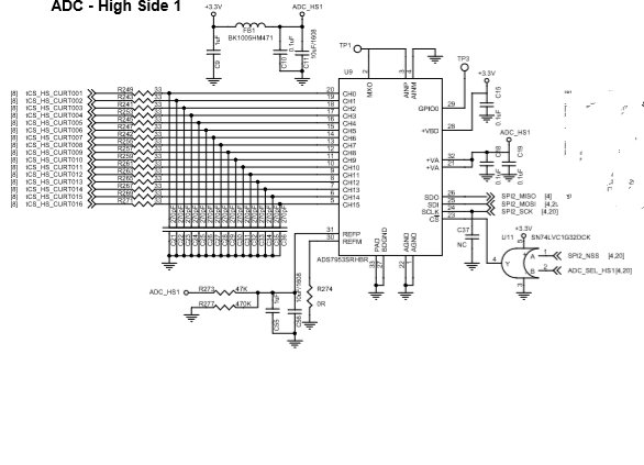
and I attached the circuit, 


  • Edmond,

    Welcome to the TI E2E forum.

    To help us get to a root cause, could you please provide the following details:

    1. Could you clarify what you mean by “some data is not correct”? Are you occasionally getting bad data or are some of the bits incorrect? Could you share a log from the DebugPrint for 20 captures?
    2. What is the sampling rate during this experiment? Does the problem go away at lower sampling rates?
    3. What is the input range and ADC_HS1 voltage? Is the resistor divider on the REFP required? Ideally this should be replaced by a reference IC?
    4. Could you please share a screenshot of the SPI interface signals (probed near the host controller) during a data capture frame?

     Thank you.

    Regards,

    Sandeep

  • Hi, SanDeep,

    Thankful for your concern,

    I updated my answers for your questions, please review it and if having more questions, please help to let me know them in early time,

    and I would like to describe our schematic, we tried to read the data of each channels of 8 ADS7953 through SPI line,

    currently, when trying to experiment : some channel connect to 3 V or 0 V directly, 

    I anticipated to read 0xfff or 0x000, but I checked only 0xfff and strange values like 0x1fff so on.... I can't check 0x000, 

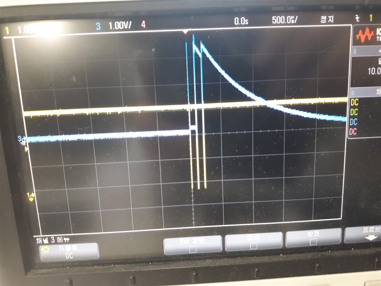
    after that, I checked the communication line of SPI, and found some problem : MISO line is strange, the waveform is not normal like the following image,

    please help to check it,

    ref) we control cs pin of each ADS7953 with 2 gpios like NSS pin and each ADC_SEL pin with OR gate, 

    thankful for your support in advance,

    1. the data can be presented in 0 ~ 4095(12 bit resolution), when checking the data, I got strange data like 

    if using below,

    change state STIMSTATE_RAMPUP -> STIMSTATE_STIMULATING, 5
    ADS7953 CH0 data is LS1: 0x089f
    ADS7953 CH0 data is LS2: 0x0899
    ADS7953 CH1 data is LS2: 0x0898
    ADS7953 CH0 data is LS1: 0x08a1
    ADS7953 CH0 data is LS2: 0x0899
    ADS7953 CH1 data is LS2: 0x1895
    change state invalid state -> STIMSTATE_STIMULATING, 6
    ADS7953 CH0 data is LS1: 0x08a1
    ADS7953 CH0 data is LS2: 0x0897
    ADS7953 CH1 data is LS2: 0x1896
    ADS7953 CH0 data is LS1: 0x089e
    ADS7953 CH0 data is LS2: 0x0897
    ADS7953 CH1 data is LS2: 0x1896
    ADS7953 CH0 data is LS1: 0x089f
    ADS7953 CH0 data is LS2: 0x0898
    ADS7953 CH1 data is LS2: 0x1895
    change state invalid state -> STIMSTATE_STIMULATING, 6
    ADS7953 CH0 data is LS1: 0x08a0
    ADS7953 CH0 data is LS2: 0x0899
    ADS7953 CH1 data is LS2: 0x1895

    I used the code as follows, 

    memset(SPI2_RX0, 0, sizeof(SPI2_RX0));
    SPI2_LS1_ManulMode(spi2_cmd0,SPI2_RX0);
    Hal_DebugPrint("ADS7953 CH0 data is ");
    Hal_DebugPrint("LS1: 0x%02x%02x ",SPI2_RX0[1],SPI2_RX0[0]);
    Hal_DebugPrint("\r\n");

    memset(SPI2_RX0, 0, sizeof(SPI2_RX0));
    SPI2_LS2_ManulMode(spi2_cmd0,SPI2_RX0);
    Hal_DebugPrint("ADS7953 CH0 data is ");
    Hal_DebugPrint("LS2: 0x%02x%02x ",SPI2_RX0[1],SPI2_RX0[0]);
    Hal_DebugPrint("\r\n");

    memset(SPI2_RX1, 0, sizeof(SPI2_RX1));
    SPI2_LS2_ManulMode(spi2_cmd1,SPI2_RX1);
    Hal_DebugPrint("ADS7953 CH1 data is ");
    Hal_DebugPrint("LS2: 0x%02x%02x ",SPI2_RX1[1],SPI2_RX1[0]);
    Hal_DebugPrint("\r\n");

    sometimes, the print sentence show the value over 4096(oxfff). like 0x3f83....so on...

    2. I tried to catch up ADC value every 1 second, the period is 1 second,

    3. ADC_HS1 is 3.3V, we used the divider resistor to set the voltage as 3.0V, what do you mean as to "Ideally this should be replaced by a reference IC?" ?

    4. I found the problem in  MISO waveform, please refer the image : I checked sclk and MISO line simultaneously, and I have a question,

    Should ADS7953 use Mode 2 of SPI communication ? which mode should use ? and how about baud rate ? I am using 2.625 Mbits/s. is it right ?

    and I am using the data to select each channels with array as follows, is it right ?

    uint8_t spi2_rst[2] = {0x00,0x40};   //reset

    uint8_t spi2_cmd0[2] = {0x00,0x10}; //CH00

    uint8_t spi2_cmd1[2] = {0x80,0x10}; //CH01
    uint8_t spi2_cmd2[2] = {0x00,0x11}; //CH02
    uint8_t spi2_cmd3[2] = {0x80,0x11}; //CH03

    uint8_t spi2_cmd4[2] = {0x00,0x12}; //CH04
    uint8_t spi2_cmd5[2] = {0x80,0x12}; //CH05
    uint8_t spi2_cmd6[2] = {0x00,0x13}; //CH06

    uint8_t spi2_cmd7[2] = {0x80,0x13}; //CH07
    uint8_t spi2_cmd8[2] = {0x00,0x14}; //CH08
    uint8_t spi2_cmd9[2] = {0x80,0x14}; //CH09

    uint8_t spi2_cmd10[2] = {0x00,0x15}; //CH010
    uint8_t spi2_cmd11[2] = {0x80,0x15}; //CH011
    uint8_t spi2_cmd12[2] = {0x00,0x16}; //CH012

    uint8_t spi2_cmd13[2] = {0x80,0x16}; //CH013
    uint8_t spi2_cmd14[2] = {0x00,0x17}; //CH014
    uint8_t spi2_cmd15[2] = {0x80,0x17}; //CH015

    and as to the setting of SPI communication, please refer below,

    hspi2.Instance = SPI2;
    hspi2.Init.Mode = SPI_MODE_MASTER;
    hspi2.Init.Direction = SPI_DIRECTION_2LINES;
    hspi2.Init.DataSize = SPI_DATASIZE_16BIT;
    hspi2.Init.CLKPolarity = SPI_POLARITY_HIGH;//SPI_POLARITY_LOW
    hspi2.Init.CLKPhase = SPI_PHASE_1EDGE;
    hspi2.Init.NSS = SPI_NSS_SOFT;
    hspi2.Init.BaudRatePrescaler = SPI_BAUDRATEPRESCALER_16;
    hspi2.Init.FirstBit = SPI_FIRSTBIT_MSB;
    hspi2.Init.TIMode = SPI_TIMODE_DISABLE;
    hspi2.Init.CRCCalculation = SPI_CRCCALCULATION_DISABLE;
    hspi2.Init.CRCPolynomial = 10;

    thanks.

  • Hello, SanDeep,

    Today I got some progress, I would like to arrange the status of this issue more for you,
    please refer the following description,

    1. I can communicate normally with ADS7953, I got the following data,
    I know that the upper 4 bit means channel number of the data that is showed together (lower 12 bit)

    ADS7953 CH0 data is LS2: 0x189e ==> 1 channel, data is 0x89e,
    ADS7953 CH1 data is LS2: 0x2898
    ADS7953 CH2 data is LS2: 0x0a75
    ADS7953 CH0 data is LS2: 0x189f
    ADS7953 CH1 data is LS2: 0x2896
    ADS7953 CH2 data is LS2: 0x097d
    ADS7953 CH0 data is LS2: 0x18a0
    ADS7953 CH1 data is LS2: 0x2896
    ADS7953 CH2 data is LS2: 0x0977

    2. but I need to check why the waveform of MISO is not normal like above image,
    Could you please kindly help to let me know the reason and the method to solve it ?

    thankful for your support in advance,

    thanks.
  • Hello Edmond,

    As described in Figure 50 of the ADS7953 datasheet, the channel requested over SDI in the n-th frame is selected by the internal mux in the (n+1)th frame and the conversion data is driven on SDO (MISO) on the (n+2)th frame.

    This can be seen in the latest log that you have shared, where the channel number in your print string and that in the data have a lag of two frames. If you want to see this behavior even more clearly, please connect CH0=0V, CH1=1.5V and CH2=3V and repeat the same experiment.

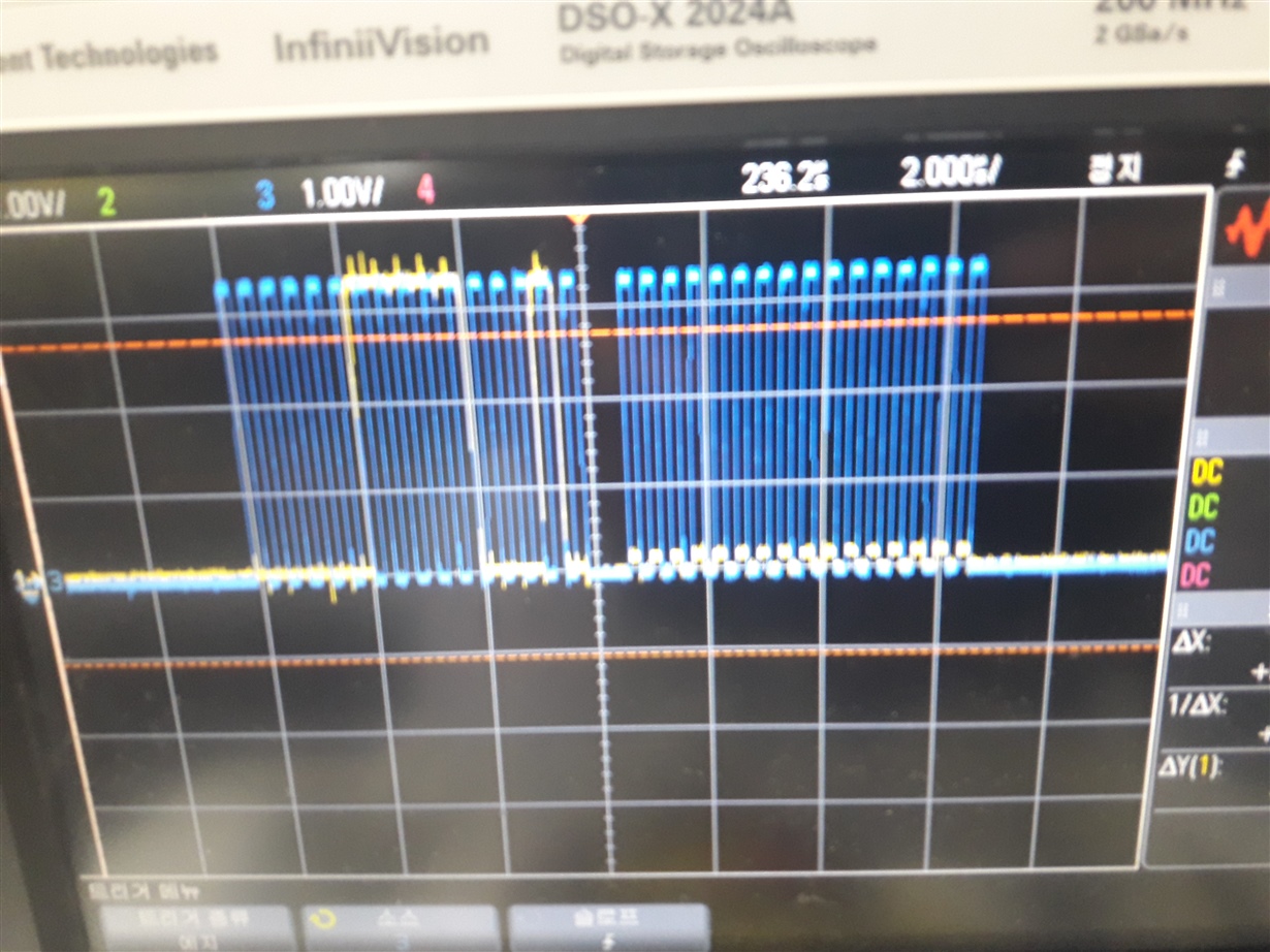
    As shown in Figure 2 of the datasheet, the data is launched by the ADS7953 at the falling edge of each clock and should ideally be captured by the host at the rising edge of the next clock. But due to trace delays or buffers in the MISO path, the time at which the data arrives at the host input pin may be different. A zoomed in screenshot of SCLK and MISO at the host pins should show us a clear picture of the interface timings.

    Regards,

    Sandeep

  • Hi, SanDeep,

    firstly, thankful for assertive support earnestly,

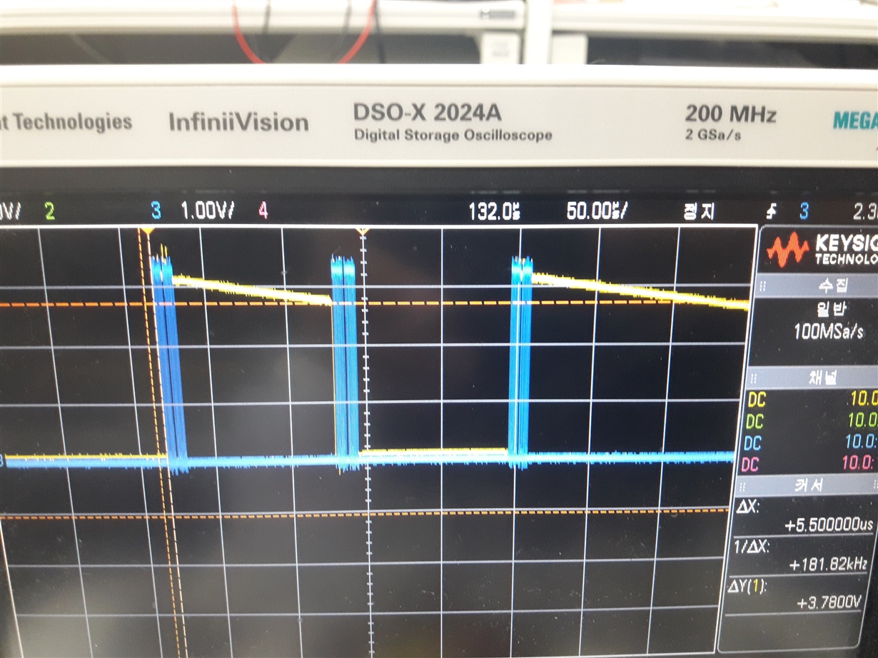
    as requested, I attached 2 image related with MISO waveform,

    one image show overall waveform including issue : MISO (yellow line) waveform is not normal,

    the other show the zoomed signal, 

    if you can find the cause of issue, please help to let me know the method to solve it with detailed information,

    and currently, I can get the exact data from ADS7953, if connecting to 0 V, got 0x000 data, if 3.0V, got 0xfff data, if 1.5V, 0x832 so on...

    and it includes the number of channel like 0x1000 : this means that the 1 channel is 0x000.

    thankful for your support in advance,

    thanks.

  • Hello Edmond,

    I am glad to hear that you are now able to read data correctly and consistently from the ADS7953.

    If you are concerned about the slow dropping waveform of the MISO line as seen in the oscilloscope plot, please refer to Fig 2 on the datasheet. The MISO line gets tri-stated after the 16th falling edge of SCLK, with delay td3. The waveform just shows the slow discharge of the voltage on the un-driven MISO line. MISO does go back to a valid voltage level at the start of the next frame, with delay td1. So what you are observing is valid behavior and will not impact the performance of your system.

    Regards,

    Sandeep

  • Hi, SanDeep,

    I will review your opinion with our H/W engineer, currently he is absent, anyway, I think that the strange waveform will not affect to read correctly the data of ADC, I am earnestly thankful for your support. I will close this issue as resolved issue,

    thanks.