This thread has been locked.

If you have a related question, please click the "Ask a related question" button in the top right corner. The newly created question will be automatically linked to this question.

Compiler/ADS8668: The SPI communication does not work

Part Number: ADS8668

Tool/software: TI C/C++ Compiler

Hello , 

I choose different channel for the ADS8668 by changing the code written into the command register and change the voltage supply for the input. 

The data of MISO is always the same. and it's a invalid data.

My code is attached below:

#include <msp430.h>


unsigned long ads8668_reg_read(void);
void ads8668_reg_write(void);

void Init_GPIO();

int main(void)
{ WDTCTL = WDTPW | WDTHOLD; // Stop watchdog timer

P1SEL0 |= BIT5 | BIT6 | BIT7; // set 3-SPI pin as second function

P2DIR |= BIT1; // CS Port
UCA0CTLW0 |= UCSWRST; // **Put state machine in reset**

UCA0CTLW0 |= UCMST|UCSYNC|UCMSB|UCCKPH;// Clock polarity high, MSB

UCA0CTLW0 |= UCSSEL__ACLK; // Select ACLK
UCA0BR0 = 0x02; // BRCLK = ACLK/2

UCA0BR1 = 0; 

UCA0MCTLW = 0; // No modulation
UCA0CTLW0 &= ~UCSWRST; // **Initialize USCI state machine**
PM5CTL0 &= ~LOCKLPM5; // Disable the GPIO power-on default high-impedance mode

P2OUT |= BIT1; 

ads8668_reg_write();

while(1)
{

ads8668_reg_read();

}
}


unsigned long ads8668_reg_read(void)
{
unsigned char SPI_RX_BUF[2];

unsigned long retVal;
retVal = 0;
P2OUT &= ~BIT1;


while((UCA0STATW&UCBUSY));

UCA0TXBUF = 0x00;

while((UCA0STATW&UCBUSY));

UCA0TXBUF = 0x00;
while((UCA0STATW&UCBUSY));
SPI_RX_BUF[0] = UCA0RXBUF;
UCA0TXBUF = 0x00;

while((UCA0STATW&UCBUSY));
SPI_RX_BUF[1] = UCA0RXBUF;
UCA0TXBUF = 0x00;


P2OUT |= BIT1;

retVal = SPI_RX_BUF[0];
retVal = (retVal << 8) | SPI_RX_BUF[1];

return retVal;

}
void ads8668_reg_write(void)
{

P2OUT &= ~BIT1;


while((UCA0STATW&UCBUSY));

UCA0TXBUF = 0xC0;
while((UCA0STATW&UCBUSY));

UCA0TXBUF = 0x00;
while((UCA0STATW&UCBUSY));

UCA0TXBUF=0x00;
while((UCA0STATW&UCBUSY));

UCA0TXBUF=0x00;
__delay_cycles(600);
P2OUT |= BIT1;
}

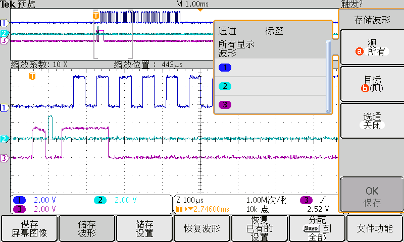
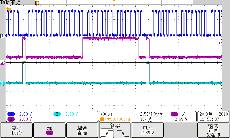
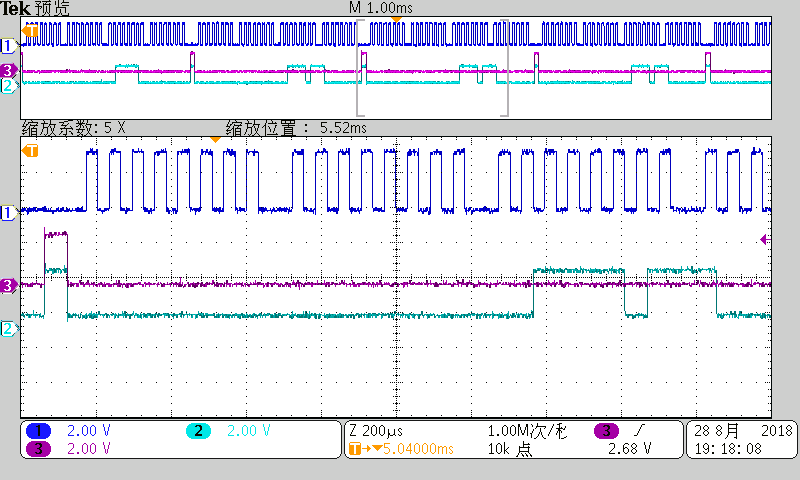
And the plot of first 32 SCLK's  CS; MOSI; CLK acquired by oscilloscope is as below:

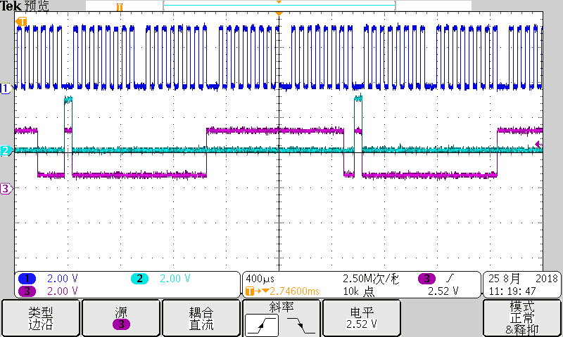
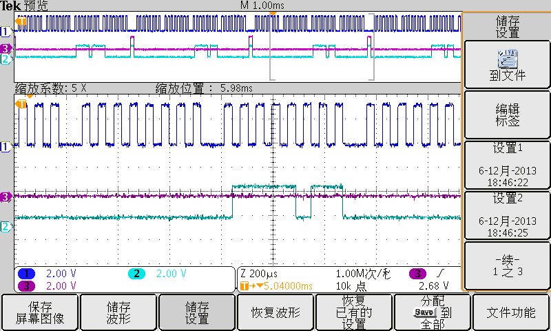
And the plot of MISO;CS;CLK is as below:

The MISO is the purple line and it won't change no matter what I do to the input. So I'm here to ask for help.

Thanks.

  • Hello Pengyu,

    I will look into it and get back to you soon. I also received Cheney's email about your same case, I will respond it as well.

    Thanks.

    Best regards

    Dale

  • Hello Pengyu,

    I hope you applied analog voltage into CH_0 because your were trying to select CH_0 by Manual CH 0 Selection command register.

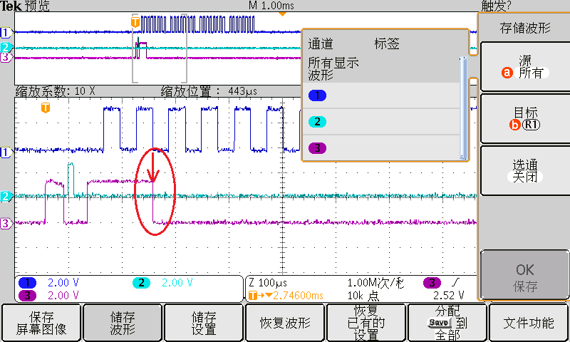
    There is one issue in your SPI timing, you were trying to send 0xC0 00 00 00" 32-bit command to the ADC, but actually the ADC will not be able to capture 0x C0 correctly because ADS8668 will latch data on the SDI line into ADC on every falling edge of SCLK (refer to Figure 1 and Data Acquisition Example in page 38 of ADS8668 datasheet for more details), based on your timing, ADS8668 can latch first bit MSB correctly which is 1, but can't lunch the second bit correctly which should be 1 as well, so the received command is 0x80 00 00 00 which is not a real command, please refer to highlighted circle as below. Please modify the phase for your SPI timing and check the code on SDO and the timing with scope again.

    Best regards

    Dale

  • Hi  Dale,

    I changed the code:.

    UCA0CTLW0 |= UCMST|UCSYNC|UCMSB|UCCKPH;   into   UCA0CTLW0 |= UCMST|UCSYNC|UCMSB|UCCKPH_0;

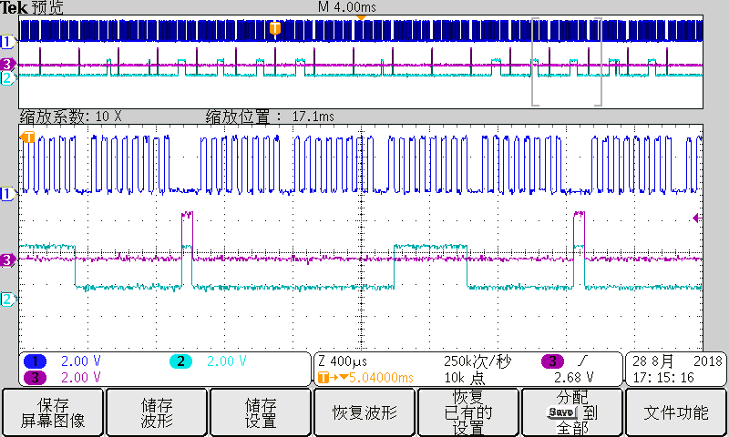
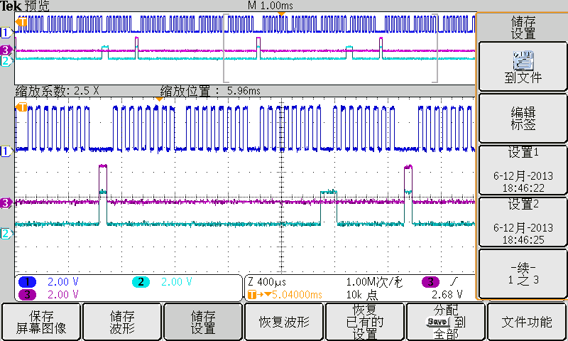
    and the first 32 SCLK becomes as followed:

    I don't know whether it is right but the second falling edge becomes a "1" ;

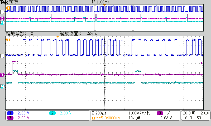
    But the out come of the SDO (ADC's) is still the same as followed:

    I also tried not to write the register and just write 0x00 into ADC, but still got the same result.

    Could you tell me what should I do?

    Thanks!

  • Hello Dale,

    I add a delay and write ' RESET' into the code:

    P2OUT |= BIT1;

      __delay_cycles(5000);

       ads8668_reg_write(0x8500);

       __delay_cycles(5000);

       ads8668_reg_write(0xC000);

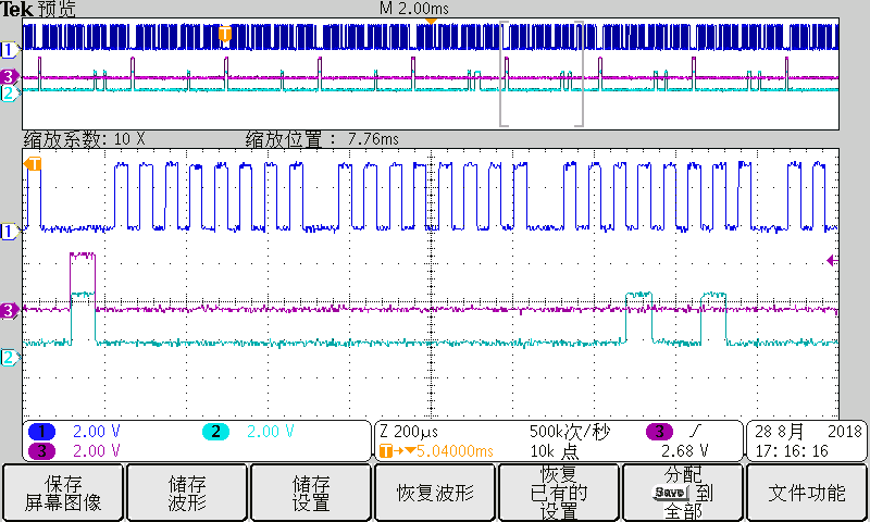
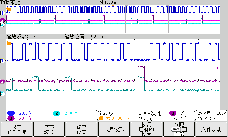
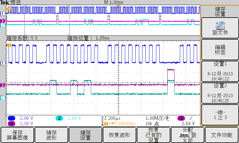
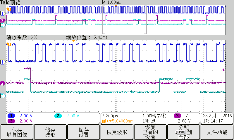
    and the SDO changes as I change the input of channel 0. But It seems like  the code of the SDO  can't match the right value(as I expect):

    When the input is 0V: (code=2032)

    When the input is 1V:(code=288)

    When the input is 2V:(code=528)

    When the input is 2.5V(code=968)

    When the input is 5V(code=1968)

    When the input is -5V(code=8)

    When the input is -2.5V(code=1024)

    When the input is -2V:(code=1184)

    When the input is -1V(code=1632)

    Above are the result I've got, But it doesn't correspond to the default set (+/- 2.5*Vref  ). It seems like the +/-5V is the max range of the input voltage.

    Could you help me to analyze ?

    Thanks!

  • Hi Pengyu,
    Can you please edit the screenshots to show which line is SDI, SDO or /CS? now I have to guess. Can you please let me know if your SPI phase is set to 1? your polarity (CPOL) is 0 which is correct. Are you using default input range without any register programming? Are you using power supply or precision signal source as an input signal ? Are you using internal voltage reference? if yes, please check if the voltage on REFIO is correct (4.096V).

    Thanks.
    Best regards
    Dale

  • Hi Pengyu,

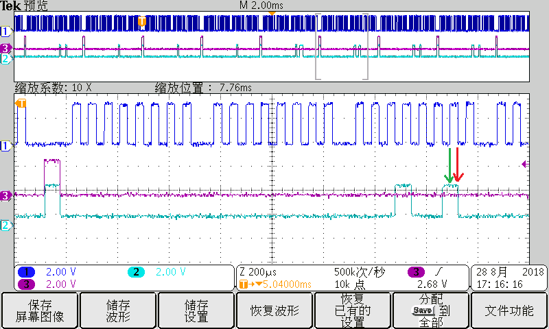
    I assume that the green line is SDO signal, check 2nd screenshots above (code=288 as you mentioned) as an example for analysis:

    Looks like the data on the SDO line is changing at the falling edge of SCLK(need a zoomed-in timing to double-check), if your host reads the data at the falling edge(red arrow), you can not be able to get stable code, if you read the data at the rising edge which is stable(green arrow), and you will get 1 at 20th rising edge of SCLK and another 1 at 23th rising edge of SCLK, so the entire data will be 00010010 00000000 (4608 decimalism) if the last 8bits data is 0 which was not shown in the screenshot. This is why need more information to check, probably your configuration for SPI interface is incorrect.

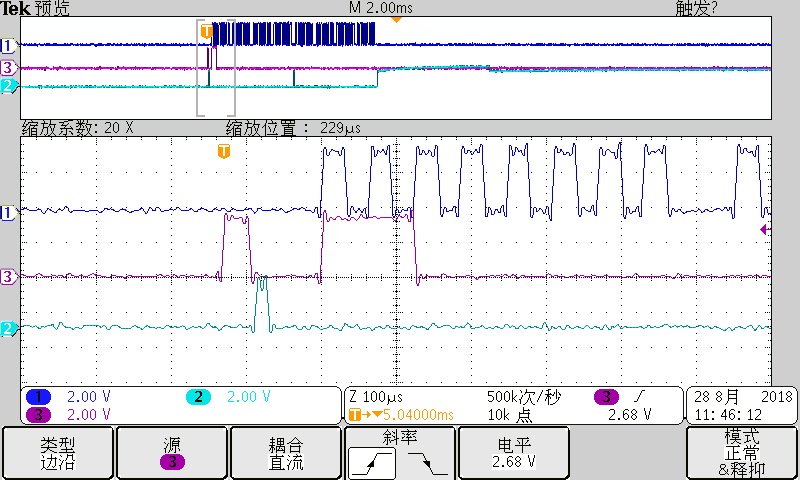
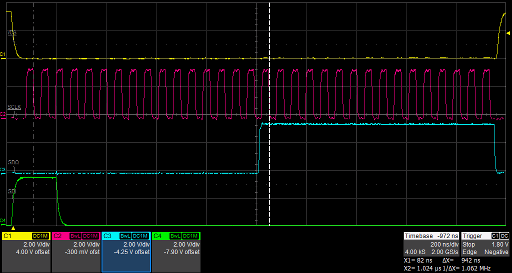
    Below 2nd screenshot is an timing example I captured on EVM board, we hope host controller can capture the data on the SDO at the falling edge, check the datasheet for more details.

    Best regards

    Dale