This thread has been locked.

If you have a related question, please click the "Ask a related question" button in the top right corner. The newly created question will be automatically linked to this question.

LMP90080-Q1: several technical questions for operating

Part Number: LMP90080-Q1
Other Parts Discussed in Thread: LMP90080, ADS124S08, ADS1248, LMP90100

Hi team

can I get your reply ?


[1] I need to calculate TUE.

     For worst TUE after calibration, I used INL = 1LSB, Offset = 15uV, Offset drift = 100nV/⁰C, Gain = 100PPM,

     and Gain drift = 0.5PPM/⁰C with Max Ta = 150⁰C,

     And finally, I found TUE is 0.826[mV]( = 5.418[LSB]).

     By using any one of BgcalMode1/BgcalMode2/BgcalMode3 without using system calibration,

     Lmp90080 can meet TUE is 0.826[mV]( = 5.418[LSB]) that I calculated for worst case ?

     We will not use system calibration.


[2] at the condition that don’t use system calibration and background calibration also,

      Customer wants to calculate TUE. What data(INL/Offset/Offset drift/Gain/Gain drift) I have to use for the calculation ?


[3] in the middle of running any one of BgcalMode1/BgcalMode2/BgcalMode3,

      Any time we can execute system calibration ?


[4] under disabling background calibration,

      If we run system calibration just only one time, such the one time calibrated offset & gain will be used forever ?


[5] what is the purpose of post calibration ?

      I cannot understand why I need it and how to use it.

      I need more explanation on SCAL_SCALING and SCAL_BITS_SELECTOR.


[6] for system calibration, CH0 ~ CH3 have their offset and gain registers by actual board level calibrated.

     CH4 ~ Ch6 will reuse the offet and gain of CH0 ~ CH2 respectively.

     So, I think the accuracy for CH4 ~ CH6 might be not best because they don’t have their actual calibrated result.

     That means, at single ended ADC, customer would better to use only 4 channels for CH0 ~ CH3 among total 7 channels

     by CH0 ~ CH6.

     How about your view on my that point ?

     Or, can we ensure IC can secure still best accuracy even for CH4 ~ CH6 at using total 7 channels single ended ADC ?


[7] for system calibration, CH0 ~ CH3 have their offset and gain registers by actual board level calibrated.

     CH4 ~ Ch6 will reuse the offet and gain of CH0 ~ CH2 respectively.

     How about background calibration which also have each offset and gain registers for CH0 ~ CH3,

     And will reuse the offet and gain of CH0 ~ CH2 for CH4 ~ CH6 ?


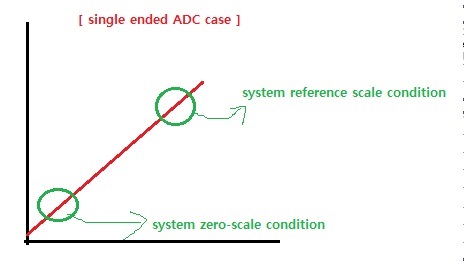
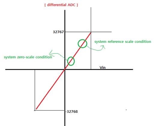
[8] at system calibration, IC needs system zero-scale condition and system reference scale condition for offset & gain calibration.

     (8-1) for single ended ADC channel, Is it OK for me to select any output code among the lower Vin range for system zero-scale

             condition as below, And to select any output code among the higher Vin range for system reference scale condition as below ?


     (8-2) for differential ADC channel, Is it OK for me to select any output code among the lower Vin range for system zero-scale

             condition as below, 

              And to select any output code among the higher Vin range for system reference scale condition as below ?


[9] burnout current is used to detect external sensor diagnostic.

      My understaning is it can detect external sensor open/short/ and so on.

      One sourcing current is from VA to VINP, and the other sinking current is from VINN to GND.

      My question is I can enable the burnout current for external sensor diagnostic regardless of differentical ADC or

      Single ended ADC ?

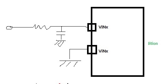
      For example, normally we uses RC filter for single ended.

      I wonder I can use the burnout current feature no matter what the H/W configuraion implemented on VINx pins ?


[10] SHORT_THLD_FALG = 1 means two VINx pins are shorted fault ?


[11] RAILS_FLAG = 1 means one of VINx pins is more than (VA ─ 50mV) ?


[12] about SAMPLED_CH bit.

        It means the channel that happens any one of SHORT_THLD_FLAG/RAIL_FLAGS/OFLO_FLAG ?


[13] at ScanMode1/ScanMode2/ScanMode3, how we can know the current read ADC_DOUT is for which channel ?


[14] about DT_AVAIL_B register.

        D/S say DT_AVAIL_B = 0 means new ADC conversion is available, and DT_AVAIL_B = 1 means no new ADC conversion ready,

       But the register map description is that 0x00 ~ 0xFE means available, and 0xFF means Not available.

       Which one is correct ?


[15] DT_AVAIL_B is “Read Only”.

        DT_AVAIL_B is cleared when MCU read ADC_DOUT ?

        I wonder when the register is cleared.


[16] at ScanMode2 with FIRST_CH = CH0 and LAST_CH = CH5, how MCU can correctly know the current ADC_OUT is for which channel ?


[17] at SDO_DRDYB_DRIVER = 00(DrdybCase1 mode), I did read ADC_DOUT completely at SDO/DRDYB pin = low.

        Then, how I can make SDO/DRDYB pin go to High again in order to detect the next ADC available ?


[18] at SDO_DRDYB_DRIVER = 03(DrdybCase2 mode), I did read ADC_DOUT completely at SDO/DRDYB pin = low.

        Then, how I can make SDO/DRDYB pin go to High again in order to detect the next ADC available ?

        Atfer done reading ADC_DOUT, SDO/DRDYB pin go to High automatically ?


[19] for Data Only Transaction, how I can make device to enter the data first mode ?

        Table 4 means using INST2 byte setting alone, I can get to data first mode and get out of data first mode ?

        Atfer done reading ADC_DOUT, SDO/DRDYB pin go to High automatically ?


[20] by PWRCH = Standby mode, ADC will be aborted. Later, if I set PWRCH = Active mode, IC will resume ADC conversion automativally ?

        Or, I have to write RESTART[0] = 1 ?


[21] in the middle of runing ADC conversion with ScanMode2, can I stop and resume ADC by sending RESTART[0] = 0 or 1 ?

        If not, how I can stop and resume ADC conversion manually ?


[22] after power-on, I send all ADC necessary registers initilzation such as CH_SCAN/CHx_INPUTCN/CHx_CONFIG.

        Then, I has to set RESTART[0] = 1 to run ADC conversion ?


[23] for example, using 3 single ended channels with ODR = 107.325 SPS for all 3 channels, the ODR per channel will be 35.775SPS(= 107.325/3) ?


[24] what about different ODR seting case for each channel ?

       For example, using 3 single ended channels with ODR = 107.325 SPS for CH0, ODR = 26.83125 SPS for CH1, and 6.71SPS for Ch2, the ODR per channel will be what ?


[25] what about different ODR seting case for each channel ?

       For example, using 3 single ended channels with ODR = 107.325 SPS for CH0, ODR = 26.83125 SPS for CH1, and 107.325SPS for Ch2, the ODR per channel will be what ?

  • Paul,


    Thanks for your interest in the LMP90080. Your post has many questions, and there's a lot of information to pull together.

    I'll be answering this in several parts, but I wanted you to know that it may take a couple of days to get through all of your questions.


    Joseph Wu
  • Paul,

    I have many of the answers that you asked for last week. The last few questions may take me a little more time to see if I can get some timing information about setting up the device.

    Paul Kim said:

    [1] I need to calculate TUE.

         For worst TUE after calibration, I used INL = 1LSB, Offset = 15uV, Offset drift = 100nV/⁰C, Gain = 100PPM,

         and Gain drift = 0.5PPM/⁰C with Max Ta = 150⁰C,

         And finally, I found TUE is 0.826[mV]( = 5.418[LSB]).

         By using any one of BgcalMode1/BgcalMode2/BgcalMode3 without using system calibration,

         Lmp90080 can meet TUE is 0.826[mV]( = 5.418[LSB]) that I calculated for worst case ?

         We will not use system calibration.

    TUE is a root sum of squares calculation of the errors for the ADC. People will often use  the typical or the min/max specifications. In your case, you've used errors for INL, offset, offset drift, gain, and gain drift which seems fair. The calculation also depends on the input range used for the measurement. If the input range is less than the full scale range, then the TUE may be smaller.

    However, you say that system calibration isn't used, and I think that the buffer is on, but I'm not sure  what gain is being used. It's a bit hard to make the calculation if I don't know all the settings.

    I would note there is a writeup about TUE in the blog posting here:

    e2e.ti.com/.../adc-accuracy-part-2-total-unadjusted-error-explained

    Paul Kim said:

    [2] at the condition that don’t use system calibration and background calibration also,

          Customer wants to calculate TUE. What data(INL/Offset/Offset drift/Gain/Gain drift) I have to use for the calculation ?

    As I mentioned, the errors from INL, offset, offset drift, gain, and gain drift are all reasonable errors. If the noise is significant  compared to these errors then I would add that too. However, based on Tables 1 and 2, the noise isn't a factor, unless the device is at gain   of 64 or 128.

    Paul Kim said:

    [3] in the middle of running any one of BgcalMode1/BgcalMode2/BgcalMode3,

          Any time we can execute system calibration ?

    For calibration, you would either set the background calibration mode to BgcalMode1, BgcalMode2, or BgcalMode3 OR you would use BgcalMode0 and then run a system calibration as described in the datasheet on pages 26 and 27 of the datasheet. If you are in BgcalMode1, BgcalMode2, or BgcalMode3 already and want to change modes, then you would first set BgcalMode0 then run through a system calibration.

    Paul Kim said:

    [4] under disabling background calibration,

          If we run system calibration just only one time, such the one time calibrated offset & gain will be used forever ?


    If you run a system calibration, this would set the CHx_SCAL_OFFSET and CHx_SCAL_GAIN registers, and these values would be retained and used for scaling the offset and gain error until the device loses power.

    Paul Kim said:

    [5] what is the purpose of post calibration ?

          I cannot understand why I need it and how to use it.

          I need more explanation on SCAL_SCALING and SCAL_BITS_SELECTOR.

    Post calibration scaling can be used to scale the output to a particular value. There may be times this is useful when processing the output data, but it can just as easily be done with a simple multiplication with whatever microprocessor you use. I don't know for sure, but  I don't think this is a popular feature.

    Paul Kim said:
             

    [6] for system calibration, CH0 ~ CH3 have their offset and gain registers by actual board level calibrated.

         CH4 ~ Ch6 will reuse the offet and gain of CH0 ~ CH2 respectively.

         So, I think the accuracy for CH4 ~ CH6 might be not best because they don’t have their actual calibrated result.

         That means, at single ended ADC, customer would better to use only 4 channels for CH0 ~ CH3 among total 7 channels

         by CH0 ~ CH6.

         How about your view on my that point ?

         Or, can we ensure IC can secure still best accuracy even for CH4 ~ CH6 at using total 7 channels single ended ADC ?

    You are correct, if you only copy the calibration registers from one channel to the next the calibration may not be the best. However, it still might be worth checking. Most channels in the multiplexer are constructed in the same way. If the customer is using the same device settings (particularly the same gain settings), the calibration settings may not be very different. In some of our other devices (ADS1248, ADS124S08), there is only one offset calibration register and one gain calibration, shared between the channels. Note that as the gain is changed, the calibration internally re-set to be accurate, but it does not change with channel changes.

    Paul Kim said:

    [7] for system calibration, CH0 ~ CH3 have their offset and gain registers by actual board level calibrated.

         CH4 ~ Ch6 will reuse the offet and gain of CH0 ~ CH2 respectively.

         How about background calibration which also have each offset and gain registers for CH0 ~ CH3,

         And will reuse the offet and gain of CH0 ~ CH2 for CH4 ~ CH6 ?

    First, there is a background calibration application note for the LMP90100, the method for calibration is the same for this LMP90080. I've put in a link for this note below:

    www.ti.com/.../snaa074b.pdf

    Read through it first, and see if it is useful. My feeling is that the background calibration is probably not useful unless the operating temperature varies a lot (maybe ±20°C?). It just depends on the change from offset drift and gain drift that is tolerable for the system accuracy. Using background calibration also requires some amount of measurement of the offset and gain to cancel it out. This may also stretch out the effective data rate so that it takes longer to make the measurement. If you only are measuring one channel, then the background offset calibration may require much more additional time, but a background gain calibration will require more time.

    Paul Kim said:

    [8] at system calibration, IC needs system zero-scale condition and system reference scale condition for offset & gain calibration.

         (8-1) for single ended ADC channel, Is it OK for me to select any output code among the lower Vin range for system zero-scale

                 condition as below, And to select any output code among the higher Vin range for system reference scale condition as below ?


    Yes, you could select two different values and use this to determine the slope and offset. The ADC INL specification is ±1 LSB max, and typical ±0.5 LSB. This means that the the line (as shown in your graph) is a straight line.

    This type of manual calibration requires some calculation to determine both values for the CHx_SCAL_OFFSET and the CHx_SCAL_GAIN. It is possible, but difficult to do this. From the ADC side, noise may be a factor. This can be made better with multiple samples and some amount of averaging. Also, you would need to take a good measurement of the input with a precision multimeter. This verifies the exact value of the ADC input. With a known input voltage and ADC output code for two different points, you can determine the slope of the line (gain) and the offset.

    Paul Kim said:

         (8-2) for differential ADC channel, Is it OK for me to select any output code among the lower Vin range for system zero-scale

                 condition as below, 

                  And to select any output code among the higher Vin range for system reference scale condition as below ?


    Doing a calibration for a fully differential ADC is a bit more complicated. In this case you might be able to make a single-ended low measurement and a high measurement to get the gain and the offset. However, I think it would be better to measure the endpoints. As before, this would take measurements for both the ADC inputs with a precision voltmeter.

    Paul Kim said:

    [9] burnout current is used to detect external sensor diagnostic.

          My understaning is it can detect external sensor open/short/ and so on.

          One sourcing current is from VA to VINP, and the other sinking current is from VINN to GND.

          My question is I can enable the burnout current for external sensor diagnostic regardless of differentical ADC or

          Single ended ADC ?

          For example, normally we uses RC filter for single ended.

          I wonder I can use the burnout current feature no matter what the H/W configuraion implemented on VINx pins ?


    The burnout current forces a small current to detect a burned out sensor. Basically, a small current is sourced into the ADC positive input, and a similar small current is sunk from the ADC negative input. If the input is high impedance (as if a sensor has burned out) then the currents pull the ADC inputs apart. This will give the ADC a large positive full-scale reading.

    With a single-ended ADC, the action is the same. Even if the negative input is grounded, the positive input should be pulled up. Note that the burnout measurements should be made separately from the normal measurement. You can't leave the burnout current always on. This is especially the case if you have series filter resistors. The filter resistor reacting with the filtering resistors will add an error in the measurement (especially if this is a large resistor).

    Paul Kim said:

    [10] SHORT_THLD_FALG = 1 means two VINx pins are shorted fault ?

    The SHORT_THLD_FLAG is set when either the SENDIAG_THLDH or SENDIAG_THLDL thresholds are crossed. Basically, if the input voltage is small, the SHORT_THLD_FLAG is set. It doens't necessarily mean that the input is shorted, it means that the input is lower than the thresholds. Figure 46 in the datasheet shows that the SHORT_THLD_FLAG comes from the status of SENDIAG_THLDH and SENDIAG_THLDL. There is a discussion on how to program the threshold values for use with the SHORT_THLD_FLAG on page 31.

    Paul Kim said:

    [11] RAILS_FLAG = 1 means one of VINx pins is more than (VA ─ 50mV) ?

    The RAILS_FLAG senses if the VINx pins is within VA-50mV and GND+50mV. This is discussed briefly on page 31. It's one of the SENDIAG_FLAGS in Address 0x19 (as is the SHORT_THLD_FLAG).

    Paul Kim said:

    [12] about SAMPLED_CH bit.

            It means the channel that happens any one of SHORT_THLD_FLAG/RAIL_FLAGS/OFLO_FLAG ?

    The SAMPLED_CH bits show the channel for which information is available in the register data. If you read ADC_DOUT, and all of the SENDIAG_FLAGS, this information is for one particular channel. The SAMPLED_CH tells you which channel the register data is for. Note, it does not tell you what channel the ADC is trying to read at the time, and the SENDIAG_FLAGS do not stay set if it is tripped. There's information in the datasheet about SAMPLED_CH on page 31, but there's also confirmation here:

    e2e.ti.com/.../564154

    Paul Kim said:

    [13] at ScanMode1/ScanMode2/ScanMode3, how we can know the current read ADC_DOUT is for which channel ?

    As mentioned in the previous answer, during the different Scanmodes you can use the SAMPLED_CH bits to indicate which channels is being read. I think that it would be best practice to read the SAMPLED_CH and the ADC_DOUT during a single 1/ODR period. This would be like Figure 48 in the datasheet, reading out the data for both between the DRDYB pulses. While there may be some overrun in read for the ADC_DOUT as shown in Figure 49, I don't think this works for the SENDIAG_FLAGS and SAMPLED_CH bytes.

    Paul Kim said:

    [14] about DT_AVAIL_B register.

            D/S say DT_AVAIL_B = 0 means new ADC conversion is available, and DT_AVAIL_B = 1 means no new ADC conversion ready,

           But the register map description is that 0x00 ~ 0xFE means available, and 0xFF means Not available.

           Which one is correct ?


    DT_AVAIL_B is really a byte and I would read the DT_AVAIL_B to check all bits. There was some original discussion about a feature to use the DT_AVAIL_B as a sample of the DRDYB at the SCLK and this might be why the datasheet discusses a single bit read.

    Paul Kim said:

    [15] DT_AVAIL_B is “Read Only”.

            DT_AVAIL_B is cleared when MCU read ADC_DOUT ?

            I wonder when the register is cleared.


    That is correct. DT_AVAIL_B is cleared when the ADC_DOUT is read. Note that this includes aborted reads. If you only read part of the data, but not all the way down to the LSB, it will still clear DT_AVAIL_B.

    Paul Kim said:

    [16] at ScanMode2 with FIRST_CH = CH0 and LAST_CH = CH5, how MCU can correctly know the current ADC_OUT is for which channel ?

    Again, this is the same answer as 13. Use the SAMPLED_CH bits to read the channel. As long as the read occurs in the same 1/ODR period, all of the registers are used for the same conversion.

    Paul Kim said:

    [17] at SDO_DRDYB_DRIVER = 00(DrdybCase1 mode), I did read ADC_DOUT completely at SDO/DRDYB pin = low.

            Then, how I can make SDO/DRDYB pin go to High again in order to detect the next ADC available ?

    See answer below 18.

    Paul Kim said:

    [18] at SDO_DRDYB_DRIVER = 03(DrdybCase2 mode), I did read ADC_DOUT completely at SDO/DRDYB pin = low.

            Then, how I can make SDO/DRDYB pin go to High again in order to detect the next ADC available ?

            Atfer done reading ADC_DOUT, SDO/DRDYB pin go to High automatically ?

    In both SDO_DRDYB_DRIVER cases, the output starts off as DRDYB and then becomes driven by SDO after the device is then read out. After the device is fully read out, it does not return SDO/DRDYB high. Note that in all cases, it is recommended that the DRDYB should be connected to an interrupt. By trying to return SDO/DRDYB high, it looks like you want to try to poll the pin.

    There may be two alternatives to what you want to do. First DRDYB may be routed to D6 which is pin 27 on the device instead of using the combined  SDO/DRDYB. This is shown on page 35 in the datasheet. Then this pin could be monitored separately as an interrupt or polled at a much higher rate. If you want SDO/DRDYB to go high, it might be worth reading something from the registers that sets the least significant bit high. In that case, I think the SDO/DRDYB pin will stay high all the way until the next data is ready. Looking through the register map, if you read one of the CHx_SCAL_SCALING coefficients for an unused, uncalibrated channel, you'll read 0x01, which should force SDO high (as long as this value wasn't previously changed).

    Paul Kim said:

    [19] for Data Only Transaction, how I can make device to enter the data first mode ?

            Table 4 means using INST2 byte setting alone, I can get to data first mode and get out of data first mode ?

            Atfer done reading ADC_DOUT, SDO/DRDYB pin go to High automatically ?


    To enter data first mode and exit data first mode, are correct in pointing out Table 4. These are the commands that you would use to enter (0xFA) and exit (0xFB) the modes. To enter and exit the mode, you issue the byte by itself. For the data first mode, you can read up to 8 consecutive registers, starting from any start address. This means that you will need to first set up the URA and LRA to the correct starting point. As in the previous questions, the SDO/DRDYB does not return high automatically, and will retain the value of the last bit clocked out.

    Paul Kim said:

    [20] by PWRCH = Standby mode, ADC will be aborted. Later, if I set PWRCH = Active mode, IC will resume ADC conversion automativally ?

            Or, I have to write RESTART[0] = 1 ?

    If you are putting the device into Stand-by mode with PWRCN=11b, then you reduce the current, but it does not completely power-down the device. As soon as you make the device Active again with PWRCN=00b, then the conversion starts up again, without having to set the RESTART bit. This was discussed in a previous E2E post, and the customer noted that the RESTART did not need to be issued. The customer was using the device in single scan mode.

    e2e.ti.com/.../1067734

    Paul Kim said:

    [21] in the middle of runing ADC conversion with ScanMode2, can I stop and resume ADC by sending RESTART[0] = 0 or 1 ?

            If not, how I can stop and resume ADC conversion manually ?


    [22] after power-on, I send all ADC necessary registers initilzation such as CH_SCAN/CHx_INPUTCN/CHx_CONFIG.

            Then, I has to set RESTART[0] = 1 to run ADC conversion ?


    [23] for example, using 3 single ended channels with ODR = 107.325 SPS for all 3 channels, the ODR per channel will be 35.775SPS(= 107.325/3) ?


    [24] what about different ODR seting case for each channel ?

           For example, using 3 single ended channels with ODR = 107.325 SPS for CH0, ODR = 26.83125 SPS for CH1, and 6.71SPS for Ch2, the ODR per channel will be what ?


    [25] what about different ODR seting case for each channel ?

           For example, using 3 single ended channels with ODR = 107.325 SPS for CH0, ODR = 26.83125 SPS for CH1, and 107.325SPS for Ch2, the ODR per channel will be what ?

    I'll check on the rest of these questions 21-25 and get back to you. I'm not entirely sure about the cases for each of these. Is background calibration used?

    Regardless look through my responses and let me know if I've misunderstood the question.

    Joseph Wu

  • Paul,


    I did check back with the original product group that developed the LMP90100 for the last questions. I was able to get a few answers.

    [21] in the middle of runing ADC conversion with ScanMode2, can I stop and resume ADC by sending RESTART[0] = 0 or 1 ?

            If not, how I can stop and resume ADC conversion manually ?


    I don't think you can stop the ADC by sending RESTART[0]=0. Instead of doing this, you could do a reset of the device then do a RESTART[0]=1. However, after a RESTART, the first sample is not valid. As an alternative, you could issue a standby command followed by an active command (this gets you back a valid first sample as described on page 38 of the datasheet). This is done through writing the PWRCN register.

    [22] after power-on, I send all ADC necessary registers initilzation such as CH_SCAN/CHx_INPUTCN/CHx_CONFIG.

            Then, I has to set RESTART[0] = 1 to run ADC conversion ?

    We weren't sure about this one. It would not hurt to write the RESTART.

    [23] for example, using 3 single ended channels with ODR = 107.325 SPS for all 3 channels, the ODR per channel will be 35.775SPS(= 107.325/3) ?

    Correct, running three different channels at the same ODR of 107.325 SPS would mean that the ODR per channel is 35.775SPS(= 107.325/3). This is described on pages 20-21 of the datasheet, with a brief description on the timing for scanning channels.

    [24] what about different ODR seting case for each channel ?

           For example, using 3 single ended channels with ODR = 107.325 SPS for CH0, ODR = 26.83125 SPS for CH1, and 6.71SPS for Ch2, the ODR per channel will be what ?

    [25] what about different ODR seting case for each channel ?

           For example, using 3 single ended channels with ODR = 107.325 SPS for CH0, ODR = 26.83125 SPS for CH1, and 107.325SPS for Ch2, the ODR per channel will be what ?


    Each channel does have ODR selection. The total scan time for all channels should be the sum of each 1/ODR. The equivalent ODR would be the inverse of that total time. For 24, this would be about 5.11SPS or about 195.6ms for all conversions. For 25, this is about 17.887SPS, or about 55.905ms.

    Hopefully this answers your questions. If you have any more, let me know, and I'll do my best to answer them.

    Joseph Wu