This thread has been locked.

If you have a related question, please click the "Ask a related question" button in the top right corner. The newly created question will be automatically linked to this question.

ADS127L01: Master-Clock vs. SPI-Clock

Part Number: ADS127L01

Hello,

I am using two ADS127L01 in daisy-chained mode with a microcontroller (STM32F7) and experiencing strange problems regarding the data I receive via the SPI bus. The MCLK is delivered via the microcontroller.

The procedure I am using is as follows:

1. Setting START pin and #CS pin low

2. Setting the master clock to 720kHz

3. Initializing the SPI to 1.6875MHz

4. Setting the #RESET/#PWRDN pin low and waiting ~3000ms

5. Setting the #RESET/#PWRDN pin high and waiting ~3000ms

6. Sending {0x41, 0x00, 0b00000001} to the ADC to set up the CRC-8 mode

7. Sending {0x20, 0x07, 0, 0, 0, 0, 0, 0, 0, 0} to the ADC to read all registers

Here I get the first errors: I am expecting returned bytes {0x83, 0x01, ..., 0x80, 0x40} from the device registers, but sometimes I get {0x00, 0x01, ..., 0x80, 0x40}. It seems that the first byte gets lost. When I lower the SPI clock the error may disappear. If I put in an extra delay between the operations it seems also to work. It looks like the first SPI clock edge has to come at the right time. Because I have to read 8 bytes (4 bytes from each device), the SPI clock has to be higher than 22.5kHz * 64 = 1.44MHz.

Let's assume the error does not appear, the procedure continues:

8. Setting START pin high

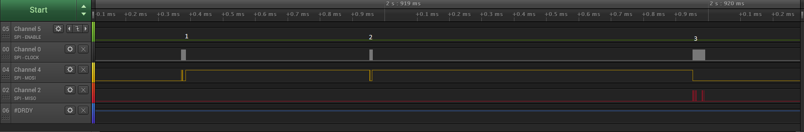
9. Start gathering data in "continues mode":

9.1 Waiting till #DRDY goes low

9.2 SPI clock rises high after ~375ns, #DRDY goes high

9.3 SPI reads 8 Bytes

9.4 After the last SPI clock cycle goes low, there are ~6.5us till #DRDY goes low

9.5 Restart from step 9.1

Here another error appears sometimes: Like in Point 7 explained, the first byte can get lost. When the error not occur, the CRC value looks fine. Because I am using the ADC's for IEPE-Sensors I can not say at the moment if the data values are valid. I will get to this part later.

For now I am interested in the correlation of the MCLK and the SCLK. But I can not find anything about that in the datasheet. Can you explain this correlation to me?

It seems like the MCLK has to be at least 0.5 * SCLK. This would mean, that with more than 2 devices I can not reach the maximum data rate in daisy-chained mode. In the datasheet, the equation 11 states that the total number of devices depends only on the SCLK.

Thanks for your help!

Greetings,

Reggie

EDIT: Sorry, I forgot to mention that all SPI read / write values are confirmed with a logic analyzer.

  • Hi Reggie!

    Welcome to our e2e Forum! Can you include those logic analyzer plots? One thing you are missing I believe is the command bytes, you need to account for those as well. The MCLK along with the data rate setting (OSR of 32 in your case I assume) sets up the period between DRDY active transitions (720kHz/32 = 22.5kHz in your setup). What happens if you boost up your SCLK to something like 2MHz?
  • Hi Tom,

    first, thanks for your answer. Of course I can include the plots.

    Just a short snippet of my software, which shows the sequence of the register write and register read:

    spiState = SpiState::WriteReg;
    u8 buffer1[3] = {0x41, 0x00, 0b00000001};
    while (!spi.Transmit(buffer1, 3))
    {
    	Thread::Sleep(2);
    }
    while (spiState != SpiState::Idle)
    {
    	Thread::Sleep(2);
    }
    Thread::Sleep(2);        // <----- LOOK HERE! 
    
    spiState = SpiState::ReadReg;
    u8 buffer2[10] = {0x20, 0x07, 0, 0, 0, 0, 0, 0, 0, 0};
    if (!spi.Transmit(buffer2, 10))
    {
    	log_err("[ADS127L01] Configuration error.");
    
    	return;
    }
    while (spiState != SpiState::Idle)
    {
    	Thread::Sleep(2);
    }
    

    Watch out for the thread delay which is commented with "LOOK HERE".


    The following plots shows a working configuration with 720kHz MCLK and 1.6875MHz SCLK.

    The first plot shows the overall sequence from startup:

    The next three plots show a detailed view of the marking "1" inside the first plot:

    Write to the option register:

    Read all registers:

    And here is a detailed view of point "2", marked in the overview plot, as you can see, everything seems correct:

    EDIT: Please ignore the MOSI-line pulled up for a few us before the conversions. I had to do some tricks with the SPI and DMA hardware of the MCU to lower the interrupt requests for the continuous data stream.


    Now I change the SCLK to 3.375MHz.

    The initialization duration is the same, here is the overview (the data gathering is not starting, because my firmware could not verify the ID of the ADC):

    The write-to-reg plot looks exactly like the upper one, except that the baudrate is faster. Now here the register read, all zeros:


    Now I change SCLK back to 1.6875MHz AND remove the delay from my software sequence:

    spiState = SpiState::WriteReg;
    u8 buffer1[3] = {0x41, 0x00, 0b00000001};
    while (!spi.Transmit(buffer1, 3))
    {
    	Thread::Sleep(2);
    }
    while (spiState != SpiState::Idle)
    {
    	Thread::Sleep(2);
    }
    // Thread::Sleep(2);        // <----- LOOK HERE!
    
    spiState = SpiState::ReadReg;
    u8 buffer2[10] = {0x20, 0x07, 0, 0, 0, 0, 0, 0, 0, 0};
    if (!spi.Transmit(buffer2, 10))
    {
    	log_err("[ADS127L01] Configuration error.");
    
    	return;
    }
    while (spiState != SpiState::Idle)
    {
    	Thread::Sleep(2);
    }


    And here now the corresponding plot of the register read:


    OSR and FILTER is set to 0 by pulling the corresponding pins low. The register value I read out confirms this.

    Thanks in advance and greetings,

    Reggie

  • Hi Reggie,

    With the Thread::Sleep(2); - how much 'delay' does that actually give you? You might be violating the td(DECODE) (see table in section 6.6), which would explain why slowing the SCLK down originally helped your situation.
  • Hi Tom,

    thank you very much for that tip. I think that should do the trick. I hadn't realize that this timing requirement is in t_clk's units. I assumed it was in ns.

    So I think that problem should be resolved :)

    Thanks again and greetings,

    Reggie
  • Let us know how you make out...
  • Hello again,

    just sending now three SPI packets, to follow the datasheet SPI rules. So the previously, randomly missing first byte is now always available.

    Overview (MCLK 720kHz, SCLK 1.6875MHz):

    The packets:

    But I've been too early pleased, when switching SCLK back to 3.375MHz I always getting zeros like before. Maybe I missed again something from the datasheet?

    EDIT: Ok, after some more testing, I have to withdraw my statement. I am getting exactly the same behaviour as before.

  • Hi Reggie,

    Rather than insert the delay between packets, can you try inserting a small delay between the command byte and the rest of the register read/write detail?
  • Hi Tom,
    which command byte do you mean? The datasheet says there are two command bytes (chapter 8.5.1.8.5) for register read / write operations.

    Greetings,
    Reggie

    EDIT: Tried to put in a delay after each command byte, same behaviour. Now sending:
    WriteReg command(0x41) - delay - {0x00 0x01} - delay - ReadReg command(0x20) - delay - 0x07 - delay - {0x00, ... 0x00}

  • How much delay do you have? With your master clock of 720kHz, you need about 5.5uS.