This thread has been locked.

If you have a related question, please click the "Ask a related question" button in the top right corner. The newly created question will be automatically linked to this question.

ADC12J1600: ADC12J1600 to TSW1400 to HSDC pro

Part Number: ADC12J1600
Other Parts Discussed in Thread: ADC12J4000, LMK04828

Howdy,

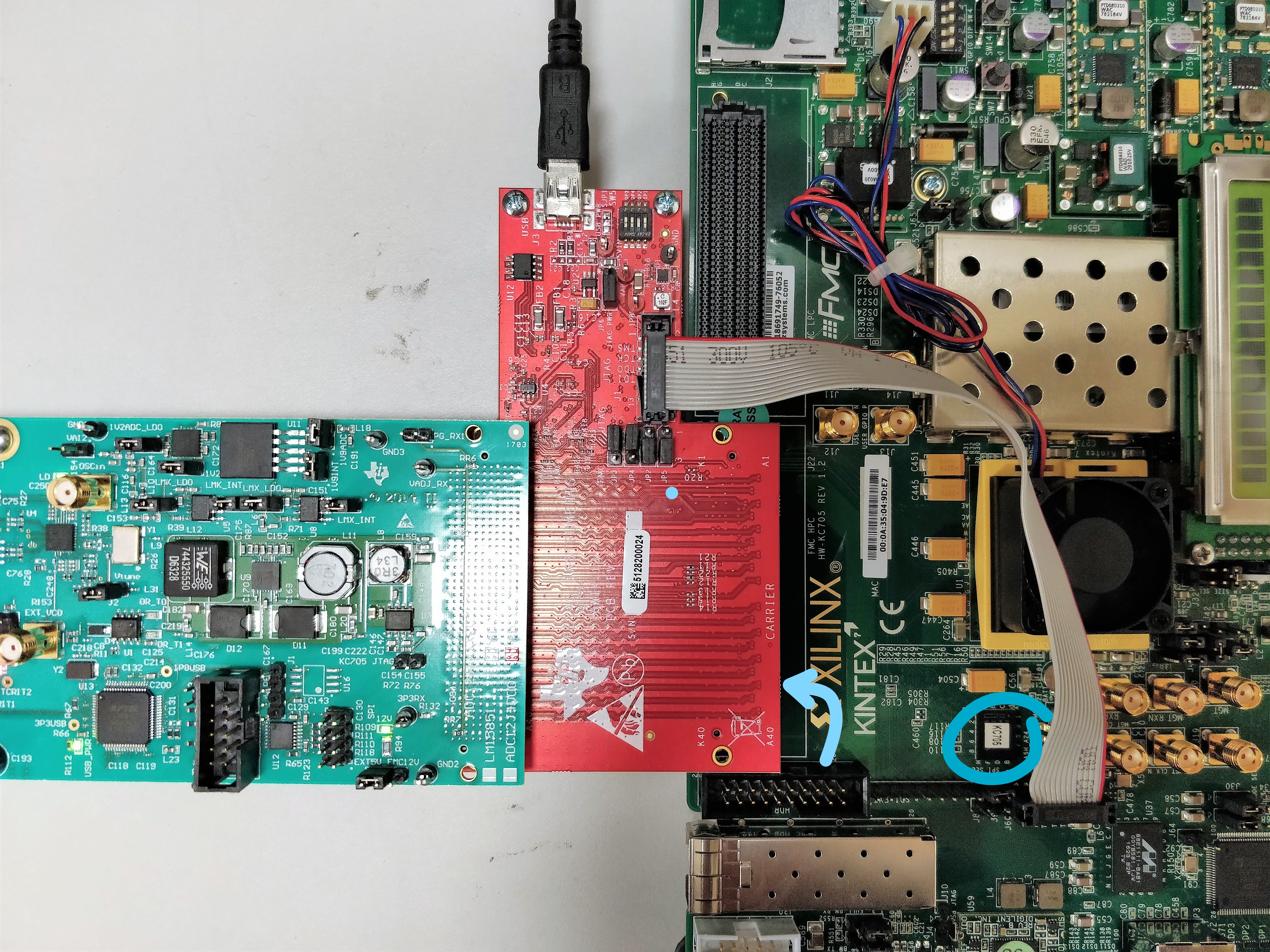
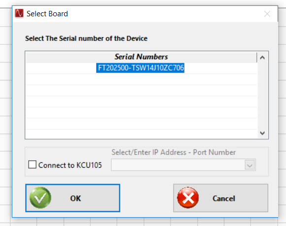
I am using the ADC12J1600 to digitize a chirp signal. I have configured the ADC and connected it to TSW14J10 (through FMC connector) and to KC705 Xilinx FPGA. When I launch the HSDC pro, it reads the TSW correctly. However, in the dropdown for ADC, I don't see an option for ADC12J1600.

Q1. How do I add that? I tried exporting settings from ADC12J1600EVM GUI and copy it there. But it is a register file and not .ini file and hence does not work.

When I try to download firmware from HSDC to FPGA, I select TSW14J10_KC705.svf but it puts out a dialog box and does not configure the FPGA. 

Could you please guide me to proceed?

  • Hi Mahesh
    Are you using a KC705 FMC carrier board, or the ZC706?
    Your post text refers to KC705, but the board and firmware names selected in the image above are for ZC706.
    The ADC12J1600EVM is compatible with the ADC12J4000_DEC_4 file you are selecting.
    For that ADC if you are setting the ADC clock rate to 1600 MHz the ADC Output Data Rate will be 400 MSPS. If you are setting the clock rate to 1000 MHz the ADC output data rate will be 250 MSPS. You may need to adjust clocks to the FPGA in the LMK04828 settings portion of the ADC GUI, but otherwise things should work fine.
    I'm not sure why you are getting that error message when loading firmware. It could be due to a mismatch if you are actually using the KC705 hardware.
    Please double check the details and I'll do my best to help.
    Best regards,
    Jim B
  • Hi Jim,

    I am using theTSW14J10 interposer card. The FPGA board is the KC705. I selected the firmware from this location -> C:\Program Files (x86)\Texas Instruments\High Speed Data Converter Pro\14J10KC705 Details\Firmware

    But somehow it appears as ZC706 in the pop-up.

    I have connected the TSW to HPC FMC port of FPGA. Is that ok? Also, I have set the jumpers J2 adn J5 on TSW on 2-3 so that JTAG is through FMC. I was tryin both JTAG options and hence te JTAG ribbon in the  picture.

    Here is my setup picture

  • Hi Jim,

    Thank you for the quick response.

    I see what you are saying. When I plug in the USB and launch HSDC pro, it shows only this device to connect to which says ZC706. Is there some setting that I need to change?

  • Mahesh,

    On the TSW14J10EVM, make sure the jumpers are set as follows:

    JP2-JP5 pins 1-2

    JP6 pins 2-3

    On dipswitch SW5, only switch 2 should be set to the "ON" position.

    Make sure on the ADC12J1600EVM, there is a shunt on the jumper labeled as "KC705 JTAG". This is located near the FMC connector.

    Regards,

    Jim

  • Hi Mahesh
    Have you succeeded in getting HSDC Pro to connect to the KC705 and download firmware?
    If not, do you have any additional information to help us debug the problem?
    Thanks,
    Jim B
  • Hi Jim,
    Thanks for following up. Sorry it took a while.

    I tried to configure it as you said but it still kept showing the same error. I guess the FTD chip on that board had some issue.
    However, I changed the TSW1410 board to a new one and it worked.
    I am now trying to read data from the ADC and plot it. Do you have a user guide/set of instructions to configure the on-board LMK as the ADC12J1600 profile is not preloaded into the HSDC GUI?
  • Hi Mahesh
    The ADC12J1600EVM needs to be configured using the GUI software for that board. That will configure the ADC and clocking devices on the EVM.
    Then HSDC Pro GUI will be used to configure the TSW14J10EVM/KC705 and control the data captures and transfer/analysis of data. The following HSDC Pro interface configuration files can be used with that combination of boards:
    ADC12J4000_DEC_4
    ADC12J4000_DEC_10
    Since the KC705 only has 4 GTX pairs only those ADC decimation modes needing 4 or fewer pairs can be utilized, DDC Bypass mode cannot be supported.
    Please let me know which decimation factor you would like to use and the desired ADC sample rate (before decimation).
    Based on that information I will recommend proper ADC12J1600EVM GUI and HSDC Pro settings for that configuration.
    Best regards,
    Jim B
  • Hello Jim,
    Thank you for the explanation. I got it now.
    I need 1000Msps data rate at the output. Since I can't decimate by 1.6 by sampling at 1600Msps, I think I need to use 1000Msps sampling and bypass mode in ADC12J1600. So, am I right in saying ADC12J4000_DEC_4 should work.
    How do we determine the number of pairs needed? Is it the L value in the LMFC?
  • Hi Mahesh

    With ADC12J1600EVM and KC705 (max 4 SERDES lanes) the highest bandwidth available will be in the following configuration:

    • ADC raw sample rate = 1600MSPS
    • Decimate By 4 Mode with DDR=1, P54=1 "Select Decimate-by-4; DDR; P54" in GUI
    • 4 SERDES lanes active at 1600 x 2 x 1.25 = 4000 Mbps per lane
    • Complex output sample rate is 1600/4 = 400 MS/s
    • Raw output bandwidth for complex samples at that rate = 400 MHz
    • Alias protected bandwidth = 400 MHz x 0.8 = 320 MHz (this is due to decimation filter cutoff bands)

    You would use the HSDC Pro device file ADC12J4000_DEC_4.

    Configure with output sample rate = 400M samples/sec.

    The FPGA clock frequencies may need to be adjusted for the Xilinx capture board. 

    In the ADC12J1600EVM GUI navigate to the Low Level View tab.

    The registers to adjust are:

    Block: LMK04828

    Register: 0x110

    The default value at LMK04828 register 0x110 after configuring the board will be 8. Change the Write Data value to 4 and then click Write Register.

    At this point the ADC EVM should be outputting the proper data and clocks to allow the KC705 to load firmware, initialize and capture data.

    Best regards,

    Jim B

  • Hello Jim,

    You are amazing. I tried this and it works. Thank you so much.

    I am trying to understand the output framing. In this output data diagram for my chosen configuration, shouldn't I0, I1, Q0.... be 12 bits?  The frame is of 16 bits as it has 2 octets implies I0 = 16bits. Or is it that the control/tail bits are not shown?

    Is this data rate at 1600/4 * 2 * 5/4 = 1Gsps? Or is it just 400Msps? Does that mean the clock is 400MHz at the output? 

    I can set my input signal to repeat at ~500KHz and I need 1000 samples per repetition => 500Msps data rate. Is 400Msps the highest I can get from this setup?

    Thanks,

    Mahesh

  • Hi Mahesh
    Once the ADC output is processed by the DDC mixer and decimation filter the output becomes complex 15b + 15b. Then an additional lsb gets added which provides over-range monitoring information, so the resulting output data in the interface is 16b + 16b.
    These complex output samples come at 1600/4 = 400 MSPS. Since these are I/Q pair complex samples the raw bandwidth is equal to the sample rate, so it is 400 MHz. The decimation filters require some cutoff transition bandwidth, so the actual usable bandwidth is approximately 320 MHz for this configuration.
    This is the best that is achievable with the KC705 capture board, since there are only 4 high speed serial lanes available.
    If you had something like the Xilinx VC707 then you could use 8 lanes and run the ADC at 1600 MSPS in DDC bypass mode. This would give an 800 MHz Nyquist bandwidth.
    I hope this is helpful.
    Best regards,
    Jim B
  • *********************************
    **Posting your answer here for continuity**

    Jim:


    Hi Mahesh
    Once the ADC output is processed by the DDC mixer and decimation filter the output becomes complex 15b + 15b. Then an additional lsb gets added which provides over-range monitoring information, so the resulting output data in the interface is 16b + 16b.
    These complex output samples come at 1600/4 = 400 MSPS. Since these are I/Q pair complex samples the raw bandwidth is equal to the sample rate, so it is 400 MHz. The decimation filters require some cutoff transition bandwidth, so the actual usable bandwidth is approximately 320 MHz for this configuration.
    This is the best that is achievable with the KC705 capture board, since there are only 4 high speed serial lanes available.
    If you had something like the Xilinx VC707 then you could use 8 lanes and run the ADC at 1600 MSPS in DDC bypass mode. This would give an 800 MHz Nyquist bandwidth.
    I hope this is helpful.
    Best regards,
    Jim B

    ********************************

    Hi Jim,

    Thank you for the explanation. I got it now. Doesn't using I & Q give us 2x BW? Or is that 400Msps the combined BW of I & Q? So, according to the frame diagram, is each lane running at 1.6Gsps? i.e. 400M/4 =100M per lane and 16b x 100M = 1.6GHz
    So, the sampling clock rate for each lane needs to be 1.6GHz?

  • Hi Mahesh
    The bandwidths I listed are for the combination of I and Q samples.
    In Decimate-by-4, DDR, P54 mode the serial bit rate in each lane is 1600 * 2 * 5/4 = 4000 Mbps.
    Each 16b sample is encoded using 8b10b encoding so there are 20 bits per sample.
    Therefore there are 4000/20 = 200 Msamples/s in each lane.
    This gives 400 Msamples/sec for I and 400 Msamples/s for Q.
    Best regards,
    Jim B