This thread has been locked.

If you have a related question, please click the "Ask a related question" button in the top right corner. The newly created question will be automatically linked to this question.

DAC38RF89: Confirming ILA_CFG

Part Number: DAC38RF89
Other Parts Discussed in Thread: DAC38J84

Hi guys,

My customer is using the DAC38rf89 in a design and has the following questions:

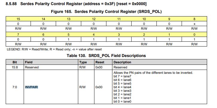
We are having some issues with the DAC38RF89 JESD interface.  We have been able to pass the PRBS tests (although needed to invert all lanes from what was expected).  Currently attempting to confirm ILA_CFG.

 Attached is our configuration of the DAC.  Questions include:

  1. Do the LID fields in the JESD ID 1/2/3  registers (0x46, 0x47, 0x48) correspond to the SERDES lane IDs (before the crossbar) or the logically mapped JESD lane IDs (after the crossbar)
  1. We have SERDES lane ID 2 mapped to JESD lane ID 0. Should LID2 be 0 or should LID0 be set to 0 if the transmitter has an ID of 0 for lane 0?
  • We have to set the SERDES inversion to the opposite of what we expect for the SERDES PRBS tests to pass and we do not currently understand why.
  • If we enable SYNC request for link configuration error (bit 5 set in JESD_SYNC_REQ register 0x51), the DAC continually asserts the SYNC line over and over and JESD alarm bit for link configuration error is set in the alarm register for all 4 lanes.
    1. If the bit is not set in the JESD_SYNC_REQ register, no alarms are reported for a link configuration error and the SYNC line stays de-asserted after initial configuration.
  1. On the TSW14J56 are you using Altera’s JESD core?
  2. Recommendations?

dac38rf89_evm_config_afterjesdreset.cfg

Regards,

Brian

  • Brian,

    We will have to take a look and get back to you.
    -Kang
  • Customer update:

    Making some progress with the DAC … have test registers supporting 4 IQ samples (verified that +/- fs/4 and DC to mixer makes sense at the DAC output). Still failing short transport layer pattern check.

    Thanks,
    Brian
  • Hi Brian,
    The short pattern transport layer testing is purely testing the transport layer (i.e. data packing layer) between the FPGA and DAC. This should be done after the phyiscal layer testing (i.e. PRBS test) over the SERDES link itself, and the link layer testing (i.e. K28.5 handshaking code test).

    I am assume the current JESD204B link is fine (i.e. link established) and therefore the customer is testing the short pattern test. If the link is not OK, then the user need to double check the link before performing the transport layer test

    There is an app note to show users the test modes for the DAC38RF8x family:
    www.ti.com/.../slaa750.pdf

    -Kang
  • Brian,

    Based on my understanding of the other similar devices, the JESD handshaking protocol is before the lane mapping cross bar. This means that the Lane ID check is checking the physical lanes. You will have to wait for Eben to confirm on this

    The SERDES inversion need to be checked thoroughly from FPGA pin out, FPGA transceiver configuration, PCB routing, and all the way to the DAC SRX lanes. The INVPAIR bit in the register map of the DAC will need to be checked

    For the JESD_SYNC_REQ register, you should at least at a minimum set to 0x03 per JESD204B standard. This will check the CGS and the 8b/10b errors to start the hand-shaking.

    If the lane ID (or part of the link configuration check ILAS) is giving you problem, you can set this register as 0x00DF to "ignore" the ILAS check. Please note this is different than "skipping" ILAS. Skipping ILAS is a sublcass 0 approach, which is not support officially in subclass 1. Ignoring ILAS simply checks the error, but ignores it. The FPGA is still expected to send out ILAS on the 2nd multi-frame after the K28.5 char stops

    The TSW14J56 is currently using Altera's JESD core, not the MEGACORE IP, I believe. We migrated to Altera a long time ago.

    My understanding is that the Altera IP always have a hard time sending out proper ILAS pattern (i.e. including Lane ID). This is the reason that we just set JESD_SYNC_REQ to 0xDF to ignore ILAS completely.

    I will ask Eben to check on the Lane ID when he gets back.

    below ppt shows the DAC38j84 sync request structure.

    -KangDAC3xJ8x JESD204B Sync Request and Error Report.pptx

  • Thanks, I will await Eben's response.

    Customer has more details as they continue to work:

    Physical layer is passing tests and don’t see any unreliable behavior but have an unexplained inversion. But we still are not passing the short pattern test. We have been able to input +/-fs/4 plus DC to the DAC with expected behavior but not consistently (I’m wondering if the startup sequence isn’t properly initializing wrt to the FIFOs). We have verified that the data is not simply inverted.

    Does the TSW14J56EVM support the mode we are targeting (LMFSHd = 42111)?

    Thanks,
    Brian
  • HI guys,

    Let me know if Eben can make a comment, on the earlier items, and if you have any response to the latest details from nov 5.

    Thanks,
    Brian
  • Hi Brian,

    1) LID are the logical lanes. These are embedded in the link configuration data that is transmitted in the 2nd ILAS multi-frame. It is not a critical parameter and I will recommend you disable link configuration checks for now to skip checking the LID

    2)LMFSHd=42111 has been tested on the TSW14J56EVM

    3) Can you confirm that the recommended startup sequence in datasheet figure 141 is being followed?

    Thanks,
    Eben.
  • 1. In response to #3 , we are currently following the sequence with the exception of not currently doing the “PLL tuning” step for the on-chip PLL (Note that we use the external DACCLK for the Serdes PLL). The PLL is locking, however, and we are validating that Bit 0 of register 0x05 is not set.

    a. This brings up another question… if the PLL needs to be tuned and it is based on temperature, does it need to be re-tuned if the temperature changes dramatically? I.e. if we tune it at start-up, will it remain locked and stable after the device heats up to normal operating temperature?

    2. We have also attempted to save the register writes from the EVM software in eval mode and play them back in our software. (Load Defaults Button -> change settings -> Configure DAC Button -> Reset DAC JESD Core & SYSREF Trigger Button)

    a. This yielded the same results as our code.

    3. Based on very limited testing, the DAC actually seems to be outputting a clean signal from the JESD data being fed from our FPGA. We just cannot seem to get the short pattern test to pass.

    a. We have signal-tap on the Altera JESD core and the data going into the core for the 128 bits of “jesd204_link_data” seem to match what we think should be there for the JESD204B short test pattern in Table 38. (For 42111, i0 of 0x7cb8 and q0 of 0xf431).

                                                                  i.      The 128 bits (based on our interpretation of the Altera documentation and based on Table 11 for 42111) is formatted as follows:

                                                                ii.      31:0  Lane 0 Data, 4 time samples of i, most-significant byte, 0x7c

                                                              iii.      63:32  Lane 1 Data, 4 time samples of i, least- significant byte, 0xb8

                                                              iv.      95:64  Lane 2 Data, 4 time samples of q, most- significant byte, 0xf4

                                                                v.      127:96  Lane 3 Data, 4 time samples of I, least - significant byte, 0x31

    b. Since we have the test pattern connected and have 4 samples, we have output DC, fs/4 and fs/2 tones by changing the IQ values and the DAC output using the NCO seems to correspond with the lane mapping described above.

    c. We have also put signal-tap in the 4 PCS instances inside the JESD core and observed the data flowing into the PCS matches the lane mapping above.

                                                                  i.      i.e. 31:0 is PCS 0, 63:32 is PCS 1, etc.

    4. Also of note: Sometimes (not consistently) we observe the following:

    a. Upon initial configuration, the DAC SYNC line de-asserts and the FPGA enters user data mode.

    b. Sometimes the SYNC line will remain stable and no alarms are ever asserted

    c. Other times, the SYNC line will periodically assert, and some lanes have bit 9 of the alarm register set (8b/10b not-in-table code error)

    5. As mentioned earlier, the SERDES PRBS tests (7, 23, and 31) all seem to pass using the Altera transceiver built-in hard prbs-generator.

    a. For some reason, however, we seem to need to set the inversion set opposite to what we think it should be. We have SERDES lanes 0,2,5,6 inverted on our board, but need to set register 0x3f to 0x9a for the SERDES tests to pass.

                                                                  i.      This may be a mis-interpretation of the datasheet. The field is named “INVPAIR”. Does 1 mean invert or does 0 mean invert? The “Reset” column of the register in the datasheet specifies “0x00” for bits 7:0 in Table 135, but those bits in Figure 139 showing the individual bits seems to indicate they should all be set (i.e. “0xff”).

    Let me know if more information will help.

    Thanks,

    Brian 

  • Hi Brian,

    1) The purpose of tuning the PLL is to ensure the PLL stays locked over temperature. Without tuning, the PLL cannot be guaranteed to stay locked over temperature
    3) Can you confirm how you are checking the results for the short pattern test? Section 2.8 of the app note below describes how the results for the short pattern test should be checked. www.ti.com/.../slaa750.pdf
    5) 1 means invert and 0 means do not invert. It is possible the serdes IP in FPGA is configured to invert the serialized data

    Thanks,
    Eben.
  • Eben,

    1. Thank you for the information. We just wanted to ensure that we would not have to periodically re-calibrate the PLL after the initial startup calibration.

    3. We have followed that procedure for checking the results of the test. (We have done this manually as our software allows us to read/write register settings from a terminal and have done it through our software on startup. See the code snippet below).

    a. Note: After the short pattern test is enabled, Bit 11 of register 0x6c is always a 1 whenever we read it. If the short pattern test is then disabled by clearing bit 12 or register 0x0c, followed by writing a 0 to 0x6c to clear any existing alarms, the next time 0x6c is read bit 11 is still a 1.

    5. We don’t see anywhere where the inversion would be occurring either in the FPGA or the schematic and layout.

    Code snippet:

    Note: Prior to this function call, the FPGA should be outputting the correct repeating pattern for the 42111 case as mentioned in the previous email.

    RegisterPageSet             = 0x09,

    RegisterAlmSysrefPap        = 0x6c,

    RegisterMultiducCfg2        = 0x0c,

    shortTestAlarmMask = 0x0800,

    bool CDacTiDac38rf89::DoShortPatternTest(uint8_t dacChannel)

    {

       uint16_t shortTestAlarm = 0x0000;

       // set page to 1 if testing internal DAC 0, set to 2 if testing internal DAC 1

       WriteRegister(RegisterPageSet, dacChannel ? 0x0002 : 0x0001);

       // Clear short test alarm

       WriteRegister(RegisterAlmSysrefPap, 0x0000);

       // Enable short test - assert bit 12

       uint16_t temp = ReadRegister(RegisterMultiducCfg2);

       WriteRegister(RegisterMultiducCfg2, temp | (1 << 12));

       // wait to see if any alarms come up and then return value of short test alarm

       std::this_thread::sleep_for(std::chrono::milliseconds(1)); // wait 1ms

       shortTestAlarm = ReadRegister(RegisterAlmSysrefPap) & ShortTestAlarmMask;

       return shortTestAlarm ? false : true;

    }

    Also, Since LMFSHd = 42111 has been tested on TSW14J56, my customer is considering get a TSW14J57 board to try and reverse engineer where their implementation goes wrong vs ours that works. Do they have access to the source code on those TSW boards? Do you have any recommendation on how to look into that in a better way?

    Thanks,

    Brian 

  • Hi Brian,

    The FPGA does not appear to be the issue here since you are able to transmit data from your FPGA to the DAC in LMF=421 mode. You can try to perform the short test pattern using TI EVM and TSW14J56 and then transfer the configuration of the DAC to your own board to replicate.
    If you need the source code for TSW14J56, you can downlaod from this link: www.ti.com/.../tsw14j56evm

    Thanks,
    Eben.
  • Eben,

    Please see below customer feedback:

    We are now passing the short pattern test.  But the spectrum is indicating a problem (as if I and Q delays are not matched).   The datasheet for the DAC doesn’t provide much insight to the internal architecture and/or associated control.  Looking for suggestions …


    Another question is the JESD RBD buffer one and the same as the JESD FIFO?


    Note: delay differences might be per JESD lane

  • Hi Randhir,

    Since this is not related to the original post this tread was created, it is better to start a new thread so that this one does not grow too long.
    Also, this recent post looks similar to the one at the link below so are they related?

    e2e.ti.com/.../2777698

    Thanks,
    Eben.