This thread has been locked.

If you have a related question, please click the "Ask a related question" button in the top right corner. The newly created question will be automatically linked to this question.

TLV2553: Output pins not going low

Part Number: TLV2553
Other Parts Discussed in Thread: ADS8339

Hello,

I'm using a TLV2553 multi channel ADC.  The output pins (data out and EOC) are connected to an analog devices level shifter P/N: ADG3304

For some reason the output pins will not drop all the way down to zero.

Here is the schematic:

And here is the waveform of the output pins.  "data out" is measured at u25 pin 16.  "eoc" is measured at U25 pin 19.

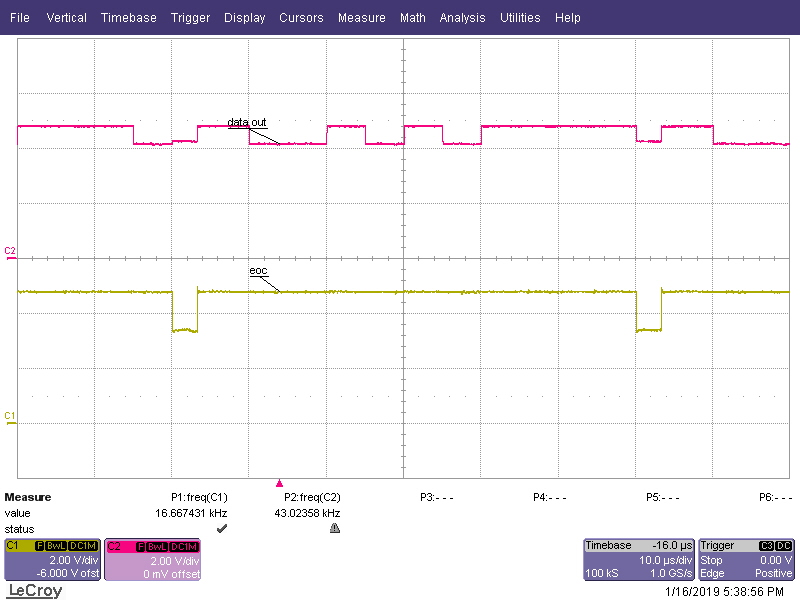
Why will these signals not drop down to zero volts in the off times?  

Note that I have also connected the output pins of another part, ADS8339, to the same level shifter (separate part) and the output pins drop to zero just fine. 

Thanks in advance

  • Hi Brian,

    Thanks for your post!

    If you look at table 6.5 of the datasheet, you will see that the Low-level output voltage is either 0.1V or 0.4V depending on your operating conditions.

    However, from your screenshot it looks like the low level is sitting around 4V - much higher than the max spec in the datasheet.

    This could be related to the output drive strength of the device, but I will have to do some additional digging to find a solution for this.

    Testing the part independently would be the best way to confirm if it's a system level or device level issue, but I'm assuming this is not easily possible for you. Give me some time and I'll see what I can do.
  • Hi Brian,

    This almost looks like a bus contention issue. Is the level shifter enabled and are the FPGA pins configured as inputs?
  • Thanks for the replies.

    The level shifter pin is high (thereby releasing the inhibit) and the FPGA pins are definitely setup as inputs.
    The problem is the signals between U25 and U27 however, so I'm not sure if the status of the FPGA pins is relevant.

    As Alex alludes to, the output pins (Y3 and Y4) are always high, as I would expect given that the input side signals never drop below the low voltage threshold. This is pretty much exactly the problem: the input pins effectively never go low, even though the ADC logic wants them to be, so the output pins are always high.

    No testing the part independently unfortunately isn't really possible.
    Please let me know what you find.
    I was thinking of adding a pull down of 100R or so on each signal line and seeing what that does.
  • Hi Brian,

    If I'm not mistaken, U27 is a bi-directional level shifter. If the Y side pins are (being driven) high (or configured as outputs), the A side won't be able to drive them below your VCCA. What are the clock, DIN and /CS lines tied to? Do they behave correctly?
  • Yes it is bidirectional, but there is no pin that selects the direction.
    After continuing to look at this on my own, the problem is probably the voltage levels. VCCA must actually be lower then VCCY and I'm violating this rule. I will have to revise.
  • Hi Brian,

    Good find! Let us know if that fixes the issue or if you have additional questions!