This thread has been locked.

If you have a related question, please click the "Ask a related question" button in the top right corner. The newly created question will be automatically linked to this question.

ADS1247: ADC measuring only AC via capacitive coupling?

Part Number: ADS1247

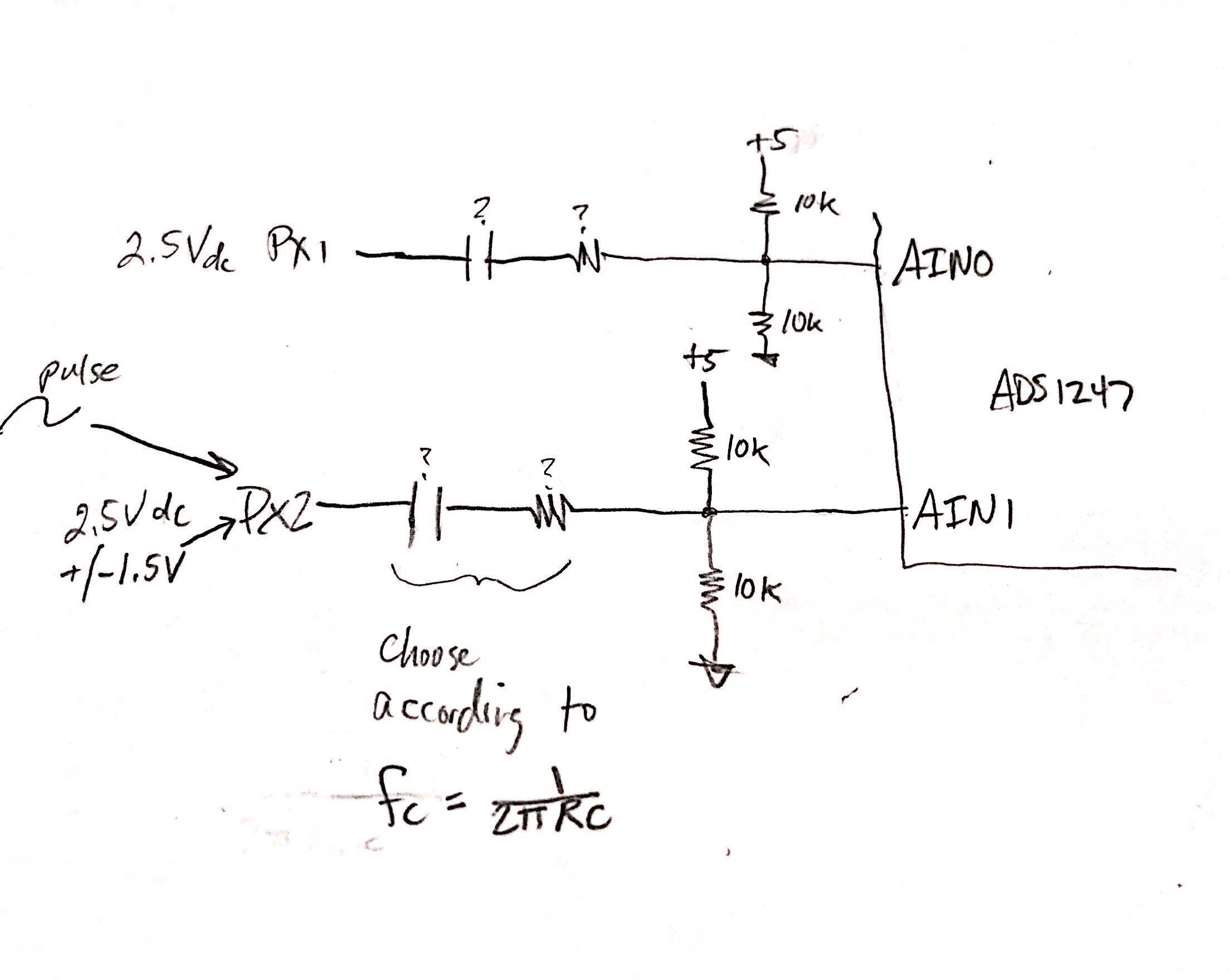
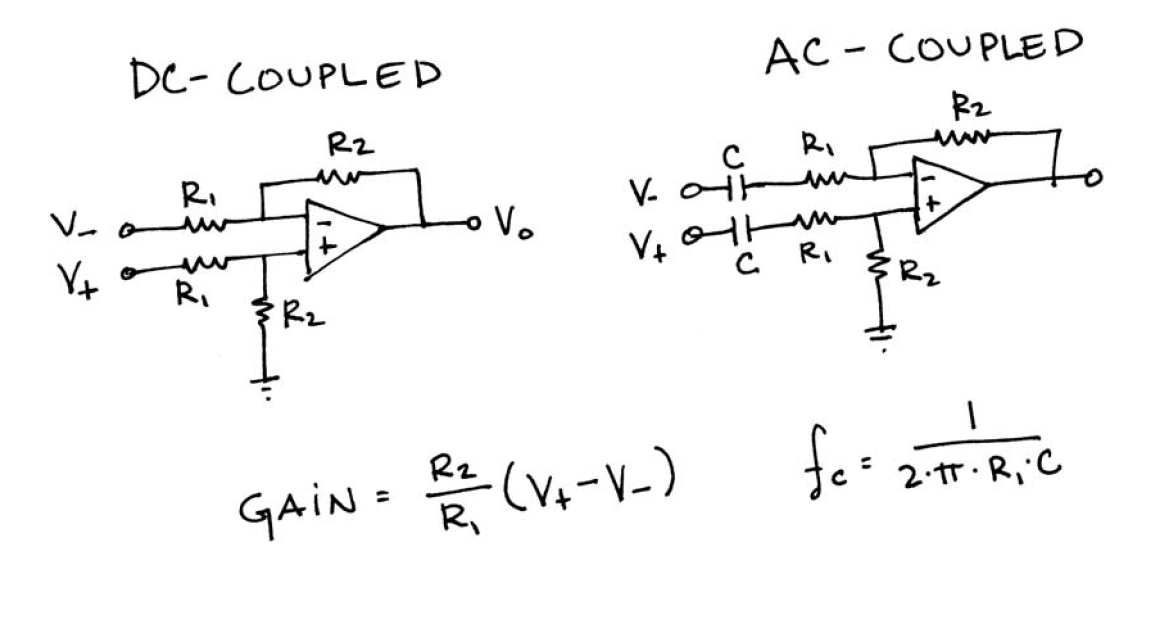
I have an application where I want to measure pulses, and the DC component is unimportant.  I do not need to measure these pulses accurately as far as magnitude.  Has anyone successfully put series capacitors feeding the ADC in a capacitively coupled architecture?   What size caps did you use? 

In my existing configuration I am measuring between a 2.5V reference and a signal that swings 2.5V +/-1.5V.  I use PGA = 1.  I have an XtoY filter on the front end, as well as low value series resistors. 

  • Hi Scott,

    Sounds like an interesting application. You may not need AC coupling - what is the general nature of the pulse(s) as far as the width is concerned?
  • Hi Tom, I'm not entirely sure, because this is a customer application, but estimating from graphs I have seen, the pulses are around 100ms wide.  The issue is, a customer using our device to measure these pulses near the noise floor of the sensor (don't care about the DC component).  The DC input into the sensor is +/-1.5 volts around a 2.5V reference, with a PGA of 1.  The pulses will ride on this DC and are very small compared to the DC.  (roughly 1/10000th).  My theory is I can eliminate the DC with the capacitive coupling, then increase the PGA gain and amplify the pulses.  I realize that the noise floor is a combination of the input noise plus the inherent noise of the ADC.  As I increase the PGA, it amplifies the noise on the input, and also the noise of the ADC.  My unknown here is whether I will get any benefit from such a system, i.e. I am trying to get a better Signal to Noise ratio to be able to detect the pulses more easily.  

  • Hi Scott,

    Tom may have an idea for a different approach (perhaps using a SAR architecture device), but your logic makes sense to me. One issue is that if and/or when you add the cap to remove the DC component, you must make sure that the input common mode is not violated as shown in section 9.3.2, equation (3). This may involve removing the DC component leaving only the AC pulses, and then adding an additional DC component to satisfy the common-mode limitations.

    Does the DC level shift or will it always be constant?

    Changing the gain of the PGA will amplify the external noise accordingly, but will not change the noise of the ADC. If you look at the noise from the output, the ADC noise decreases proportionally to the external noise on the input as you increase the gain.

    External noise on input -> PGA -> ADC (+Noise) -> Output
  • Thanks Alexander I appreciate your helpful response.....I'll look forward to Tom's response if he has a different approach.

    Time to market is a factor here, so unfortunately I can't change my ADS1247 to something else at this point.

    If both my 2.5V reference signal (PX1 on my schematic) and my 2.5 +/-1.5V signal (PX2) is isolated by a capacitor, I'm thinking that the DC component does not make a difference, as a capacitor becomes like an open circuit to DC.  So the ADC will see open on both leads with a pure DC signal, and the common mode AC noise will cancel as long as the input impedances are equal.  Then the pulses (which only occur on PX2) will be sensed by the ADC. Similar to AC coupling an op-amp. I believe that the magnitude of the pulse will be seen by the ADC as centered around 0V DC, so I will still need to bias both inputs with a weak resistor divider to 2.5V to keep a valid common mode input range. This will also prevent a floating (high impedance) input situation in the absence of any AC.  I attached a jpg with what I think I would need on my inputs, with the series capacitor and resistor TBD based on the corner frequency.  Thoughts?  I'm wondering about keeping a very small capacitance in C9-11 to filter the "grass" in common and differential mode ranges. 

    By the way, I use the internal reference of the ADC in this application. I attached portions of my schematic. Pay no attention to what is attached to pins 5-7, and 11-12... this is only populated in another application on another BOM. AVDD (off page) is tied to +5V with 10uF and 0.1uF caps to AGND.

     .

  • Hi Scott,

    Happy to help!

    Your first figure shows a CR high pass filter where the two 10k resistors are in parallel which is equal to 5k. The resistor with a ? value will equivalently be in series with the 5k resistance. I recommend removing this resistor.

    R = 5k

    Since you said that the pulse width is around 100mS, I took that to mean that the pulse is around 10Hz. Rule of thumb for filter design is to put the cutoff frequency a decade before the signal frequency for highpass, or a decade after for low pass. Since you are designing a high pass filter, this means that the cutoff frequency should be ~1Hz.

    fc = 1Hz = 1/(2*pi*R*C) ~=~
    C = 1/(2*pi*R*fc) = 1/(2*pi*5k*1Hz) = 31.8uF
    A 32uF cap should be fine.

    Make sure that the capacitor voltage level is capable of handling the DC that it will be coupling out.

    I attached a TINA schematic that may be helpful if you want to run some simulations. 

    HP_CR_Filter.TSC