This thread has been locked.

If you have a related question, please click the "Ask a related question" button in the top right corner. The newly created question will be automatically linked to this question.

ADS8568: Configuration register doesn't read-out and AD code out by a factor of two

Part Number: ADS8568

Hi,

I have two issues but perhaps related in that they involve reading from the device.

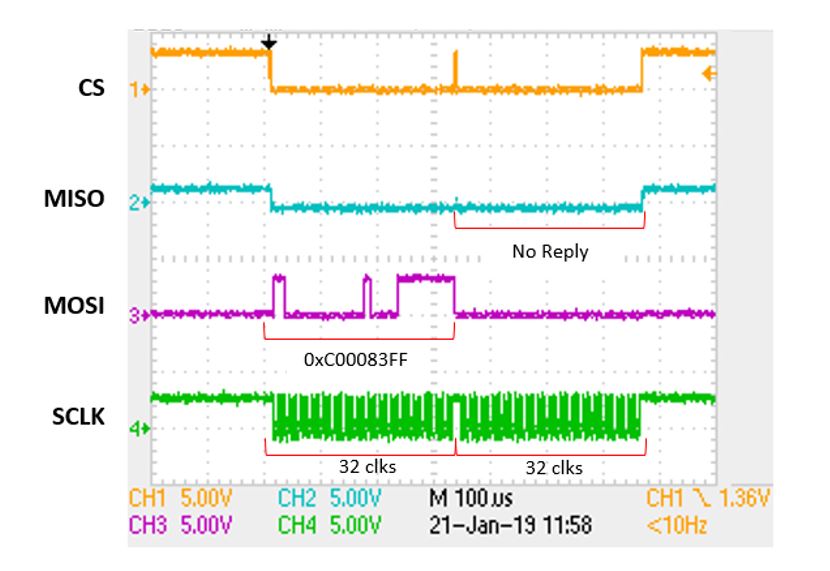
The first issue is that the CONFIG register doesn’t read-out. The READ_EN bit is set in a write to the configuration register but there is no reply, as shown below. (The write to the CONFIG register is successful as Vref can be setup and observed on pin 56. Vref can be changed from 2.5V to 3V.)

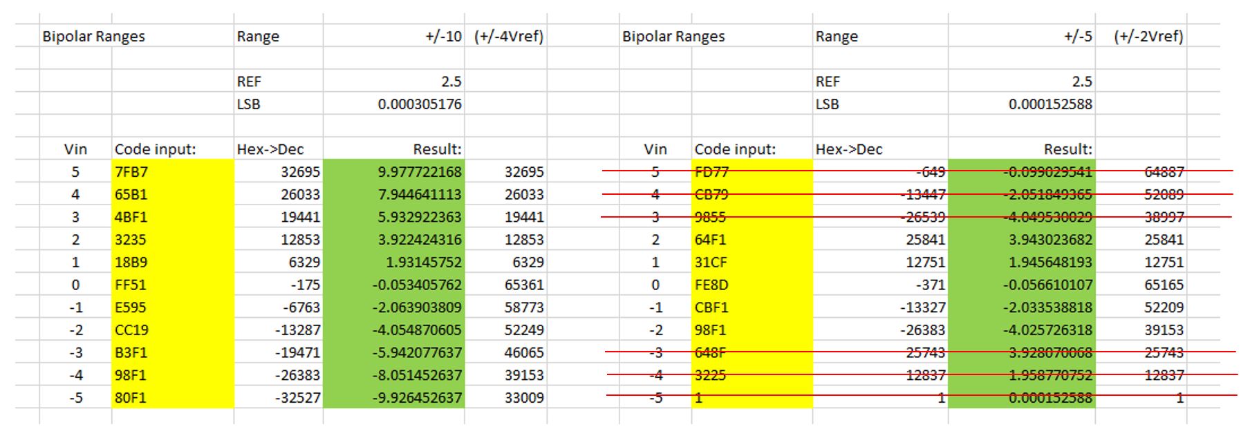
The second issue is that the A/D conversion codes returned are a factor of 2 from the input voltage.

i.e. with Vref at 2.5V

using a x4 range, a -5V to +5V input range is returned as -10V to +10V (voltage from code equivalent)

and using a x2 range, a -2.5V to +2.5V input range is returned as -5V to +5V (voltage from code equivalent)

Returned codes are saturated beyond these inputs. Although changing the scales shows that the ranges can be changed I expected that an x4 range would have accepted a -10V to +10V input and an x2 range would have accepted a -5V to +5V input.

(All dc voltages)

Regards,

  • Hello Joseph,
    I have responded your direct email with questions on 1/18, I hoped you can post your next query to E2E next time.
    For your first question, after you sent command(0xC00083FF), did you activate conversions by CONVST_x?
    For second question, what is your configuration for polarity and phase of SPI? it will be helpful if you can upload a data reading timing plot for /CS,SCLK,SDO and SDI (Figure 1).

    Regards,
    Dale
  • Hi Dale,
    Yes, thanks.
    I didn't appreciate that CONVST_x needed to be activated in order to return the configuration register - now working.
    Spot on - I have got by for so long in setting up devices without adjusting the SPI configuration that I hadn't thought of that.
    Cheers,
    J Murray
  • Hi Joseph,

    Thank you for your feedback. In case other engineers will have a similar query about ADS8568, I summarized following two points:

    1. Internal Configuration register reading:  

    ADS8568 needs two accesses (conversions activated by CONVST_x) to output Configuration Register contents to SDO_A line. Please refer to the description for Bit 30 of Configuration Register in Figure 44 of datasheet. 

    2. SPI communication:

    Regarding the serial timing in Figure 1 of ADS8568 datasheet, SCLK level is '1' for idle status, so the clock polarity CPOL=1, the ADC will latch or read data at the falling edge of SCLK which is the first edge, so clock phase CPHA=0.

    Regards,

    Dale