This thread has been locked.

If you have a related question, please click the "Ask a related question" button in the top right corner. The newly created question will be automatically linked to this question.

ADS1261EVM: AC excitation and connector J5

Part Number: ADS1261EVM
Other Parts Discussed in Thread: ADS1261

I am trying to do AC excitation on this board. Am I supposed to use connector J5? Also, is the included AC excitation the logic and you have to provide the means to drive (like the included bridge driver), or can you do this with the chip only and no driver?

  • Well, it says in the datasheet that it needs external components. Now my only issue is that I cannot get this thing to read. When ever I try to run the data analysis, it just says that there is no data and nothing really updates at all.

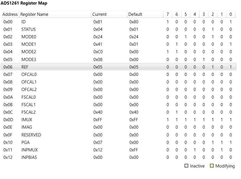
    Here is my reg map. 

  • Hi Andrew,

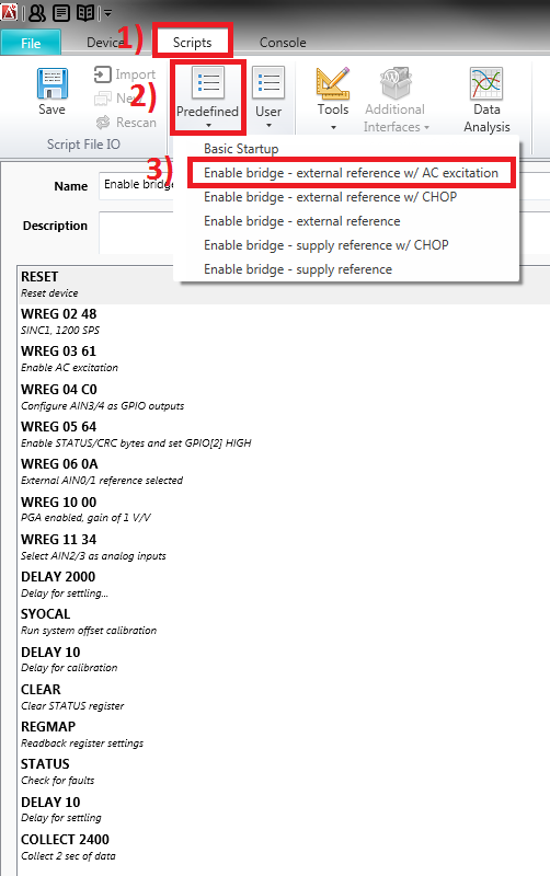
    Try using the included AC Excitation script to configure the ADS1261...

    If you use this configuration, then J5 will output alternating +/-5V excitation voltages. U1 (on the bottom side of the board) is the driver.

    You can use this voltage to excite your bridge, but you'll also need to wire the EXC_OUT+ signal to AIN0, the EXC_OUT- signal to AIN1, and then the bridge outputs to AIN2/3. In the above script the AIN0/1 pins are used as an external reference and the AIN2/3 pins are the analog input that gets sampled.

    Let me know if that helps!


  • NOTE: I made a small correction above. The excitation voltage is always 5V (it's shared with AVDD and AVSS), but the polarities are switched from +5V to -5V in ac-excitation mode.

    The script should help you configure the GPIO pins and the correct AC excitation mode. Note the EVM uses an alternate 2-wire ac-excitation mode. In the register map you'll see that the device is configured for 4-wire mode, but only GPIO2 and GPIO3 are enabled.

    Once you get the configuration working, feel free to go back to the register map and increase the PGA (the script only programs the PGA gain to 1 V/V).

  • Thanks! It worked. If I wanted to shrink the Full Scale span to get more counts out of the ADC (I have a small input span), I could just change the reference voltages that go into AIN0 and AIN1, correct? Of course, doing so may add noise since everything would no longer be on the same supply....
  • Hi Andrew,

    You certainly can adjust the reference voltage...

    Sometimes excitation voltages greater than 5V are applied to the load cell to increase the output voltage; however when using larger excitation voltages, the reference voltage needs to be divided down to 5V or less. While increasing the signal amplitude, this starts to break the ratiometic relationship between excitation voltage and reference, and if the voltage is increased enough you'll start to see self-heating effects within the load cell.

    Making the reference voltage smaller for the purpose of decreasing the LSB size and increasing the code counts, works when your resolution is limited by the quantization noise (i.e. the LSB size). However most high-resolution delta-sigma ADC's do not provide full 24-bit noise free performance because of thermal noise level that exceeds the quantization noise. In this case, when the LSB size is decreased you'll see the noise (as a number of codes RMS or peak-to-peak) increase (the noise level remains the same, but the code counts will increase as the LSB size decreases) since the thermal noise is not affected by the reference voltage or LSB size. For this reason I would recommend trying to keep the reference voltage matched to the excitation voltage as much as possible, otherwise it introduces an additional source of noise into the circuit.