This thread has been locked.

If you have a related question, please click the "Ask a related question" button in the top right corner. The newly created question will be automatically linked to this question.

ADS8910B: Setting ADS8910B to Quad-SSI mode with MSP432E401Y

Part Number: ADS8910B
Other Parts Discussed in Thread: MSP432E401Y, ADS8900B

The recommended method for setting the ADS8910B to quad-SSI mode with the MSP432E401Y is to first configure the MCU SSI port for 4-wire SPI and write to the ADC's configuration register, then configure the MCU SSI port for quad-SSI mode. The MSP432E401Y recommends against switching from legacy SSI to quad SSI mode: 

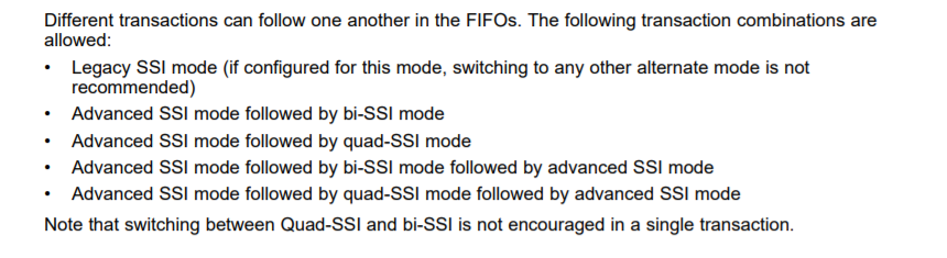
Is a one time switch from 4-wire SSI to quad-SSI acceptable despite this warning? Would it be better to use separate SSI ports on the MCU for the initial 4-wire SSI ADC configuration, and the quad-SSI data retrieval?

For the hardware implementation of this method, the MSP432E401Y's SSI_Tx is shared with the quad-SSI XDATA0, so the SDI and SDO-0 pins on the ADC8910B would need to be tied together. Will this cause any issues on the ADC end? Is the SDI pin ignored by the ADC when it is outputting data on the SDO-0 pin? 

  • Hi Michael,

    You will need to use separate MSP432 pins for the SDI and SDO-0 pins. The ADS8910B captures data on the SDI pin at the same time as outputting conversion data or register data on the SDO-x pins.

    I am not familiar with the MSP432 and the QSSI, but you will probably need to use separate SSI ports, one to handle the standard SPI and the other to handle the quad-lane data. I need to check with the MSP432 support team and will reply back when I have some answers.

    Regards,
    Keith N.
    Precision ADC Applications
  • Hi Michael,

    It will be later next week before we can get specific feedback regarding the MSP432 and the use of the QSSI peripheral to support 4 lanes of data. However, I do want to point out that a single lane, standard 3-wire SPI interface, can handle the maximum 1Msps sample rate of the ADS8910 using a 20MHz SCLK, so this would be an alternative as well.

    Regards,
    Keith
  • Hi Keith,

    Thanks for the response. According to the 8910B datasheet, a standard 3-wire SPI would require a 58MHz SCLK (18-bits in 300ns acquisition window), but using the device's enhanced-SPI would allow that to be reduced to 20MHz. I believe implementing the enhanced-SPI would require an FPGA, which is why I want to use the QSSI interface, to reduce the SCLK requirement to ~15MHz at 1Msps.
  • Please keep me updated on the MSP432 team's feedback, but it seems that if I need to separate the SDI and SDO-0 pins on the ADS8910B, then I don't have any other option than to use separate SSI ports on the MSP432. In this case, I believe I can tie the CLK and CS of the two separate SSI ports together and connect the SSI_Tx of one port to the ADC SDI, and the quad data lanes of the other SSI port and ADC together.
  • Hi Michael,

    I think you are correct; you will need to configure two of the SSI ports if you want to use 4 lanes for SDO.

    Enhanced SPI on the ADS8910B consists of multiple options; increasing the width of the output data bus (quad SDO) is just one of three options. The 20MHz SCLK shown on the first page of the data-sheet does not depend on using 4 lanes of data, but using the extended data transfer window; discussed in section 7.5.3 of the datasheet. This feature can be implemented using a standard SPI interface by clocking data in the Zone 2 region as shown in Figure 46 of the datasheet.

    By choosing when to assert /CS low to clock the data out of the device, you can increase the time available up to the full conversion cycle time minus 50nS. So, for 1Msps sample rate, you have 950nS to clock the data out. For 18b (you do not need to clock the additional bits), you need a minimum SCLK of about 1/(950ns/18)=19MHz. There is some additional setup time, which is why the datasheet suggest 20MHz as a nice round number. The point is that by clocking data out in the Zone 2 region, you can use a standard SPI port with a single SDO line at 20MHz SCLK rate and support 18b data at 1Msps.

    The only tradeoff when using Zone 2 is the response time is longer, which may be an issue if you are using the part in a digital control loop.

    I hope this helps clear things up a bit.

    Regards,
    Keith
  • Section 7.5.3 in the 8910B datasheet suggests using a data transfer window of almost the whole cycle time, excluding the time right before a start of converstion: tqt_acq + td_cnvcap. Section 2.1 of this TI white paper: http://www.ti.com/lit/wp/sbay002/sbay002.pdf explains that there is a critical window near the end of a conversion where any digital noise can impact the LSBs being computed at that time. The suggested workaround in the whitepaper is using the ADC's source-synchronous mode to generate a STRB signal that freezes during the critical silent zones, and that the host SPI controller can use to clock in the data. 

    Implementing this with just the MSP432 MCU would seem to require 2 SPI ports, one as a master to provide the SCLK and configure the ADC, and one as a slave to clock in the output data with the ADC's strobe. The MSP432 datasheet specifies that the SSI CLK in slave mode must be 12 times slower than the system clock, limiting the max clock rate to 10MHz (the max clock rate in master mode is 60MHz). Because of this limitation it seems that an FPGA would be required to implement source-synchronous mode. Would there be any other way to implement this method with just the MSP432 MCU?

  • Hi Michael,

    The TI white paper you refer to was written before we had SNR data for several of the ADC's using this feature. The parts can meet SNR specifications when following the Zone 2 guidelines in Figure 46 of the datasheet. For the ADS8910B you have 950nS in Zone 2 to transfer the data without degrading results.

    I checked the performance on the ADS8900B EVM (20b version of the ADS8910B), and it showed no degradation when going from Zone 1 to Zone 2. I also verified that it used about 800nS of the 950nS window to transfer the data.

    I hope this helps.

    Regards,
    Keith
  • Hi Michael,

    You can use the standard SPI on your MCU and the Zone 2 feature of the ADS8910B to meet your throughput requirements.

    We are looking at using the QSSI feature on the MSP432 to support the Quad-SDO feature of the ADS8910B, but this will take some time, and I do not have an estimate when it will be complete.

    I am going to go ahead and close this post, but if you have further questions, feel free to reply or open a new thread.

    Regards,
    Keith
  • Thank you for all the help and clarification on the Zone 2 feature! We are working on getting the QSSI interface going on the MSP432, I will can update this post if we are successful.