This thread has been locked.

If you have a related question, please click the "Ask a related question" button in the top right corner. The newly created question will be automatically linked to this question.

ADS1256: Noise Coupling between ADC channels

Part Number: ADS1256

Hi Chris,

I am collecting data of 2 ADC channels on the ADS1256. The below are the images of the two separate trials

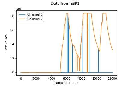
The first channel I connect it to ground, the second channel I connect it to a PSU and I change its output voltage. As you can see, the noise is coupled between the two channels. The plot shows that the noise amplitude of the first channel (GND) is capped by the profile of the second channel (PSU voltage).

I wonder what might be the cause of this problem.

Thanks,

Khoi Ly

  • Hi Khoi,

    Is hard to say what might be be happening without fulling understanding your input circuitry. If you have schematic you could share it would be helpful. Unfortunately, I was not able to access the google drive link you posted in a previous thread.

    From first glance it looks sporadic cross-talk or data corruption. Some possible causes may include:

    • Data formatting. The jumps from 0 to full-scale could be from treating the data as unsigned. The ADS1256 produces signed data, so its very common to see data around 0xFFFFFF (-1), 0x000000 (0), 0x000001 (1). If not converted to a signed decimal value then it may look like the data is jumping between zero and full scale.

    • Reading data before a conversion has completed. If data is read and re-read before the /DRDY falling edge, then you may be getting the same conversion result duplicated on both channels. Since CH1 and CH2 tend to jump to the value of the previous channel you might be reading the same data twice.

    Also seeing CH2 max out the ADC's input range has me a bit concerned how high the input voltage to CH2 is actually going. Do be sure that the PSU voltage and current is limited so as not to damage the ADC. Current should be limited to 10mA in case of over-voltages.

    I'd recommend trying a couple of different tests for troubleshooting...

    • Try measuring a single channel without multiplexing and seeing if this behavior is still occurring. If it goes away, then likely it is a digital issue. If it doesn,t then there might be some kind of cross-talk or real analog effect.
    • Try using a slower data rate and see if the error goes away. If so then it might be related to data corruption.
    • Keep the voltage on CH2 constant and see if the cross-talk occurs with only a DC signal.

  • Hi Chris,

    When I reduce the sampling rate 5 times slower, the coupling signals between two channels disappear. I think it is the data corruption then.

    for (i=0; i<=5; i++) {          // read all 6 single ended channels AIN0, AIN1, AIN2, AIN3, AIN4, AIN5
    				while (gpio_get_level(PIN_NUM_DRDY) == 1) {} ; // Wait until the data read pulls LOW
    				// Switching between channels
    				reg = 0x01;  cmd = 0x00; data = mux[i]; // 1st Command Byte: 0101 0001  0001 = MUX register address 01h
    
    				ADS1256_REG(spi, reg, cmd, data); // Data Byte(s): xxxx 1000  write the databyte to the register(s)
    
    				//SYNC command 1111 1100 (0xFC)
    				cmd = 0xFC;
    				ADS1256_cmd(spi, cmd);
    
    				//WAKEUP 0000 0000
    				cmd = 0x00;
    				ADS1256_cmd(spi, cmd);
    
    				// Read Data
    				cmd = 0x01;
    				ADS1256_cmd(spi, cmd); // Read Data 0000  0001 (01h)       // ********** Step 3 **********
    
    				adc_val[i] = ADS1256_read(spi);
    				adc_val[i] <<= 8; //shift to left
    				adc_val[i] |= ADS1256_read(spi);
    				adc_val[i] <<= 8;
    				adc_val[i] |= ADS1256_read(spi); 
    }

    I wonder where in the above code snippet that has the DRDY issue? I could look into the logic analyzer and setup a delay appropriately.

    Thanks,

    Khoi Ly

  • Hi Khoi,

    I don't see anything inherently "wrong" about the code. It could just be that polling /DRDY and reading data is not occurring fast enough on the MCU to keep up with the higher data rates of the ADS1256.

    How fast is your SPI SCLK, and are you able to increase the SCLK frequency at all? NOTE: SCLK can only go as fast as fCLK/4 (or 1.92 MHz for a 7.68 MHz ADC clock).

    Are you able to use a /DRDY interrupt to read the ADC data. Polling a GPIO pin ()hardware) may take longer than polling for an internal variable that gets set during a hardware interrupt.
  • Hi Chris,

    In a previous thread, you mentioned that the fastest clock rate of ADS1256 is Fclock/2 which is ~3.4MHz; what does it mean by SCLK =1.92MHz in your reply?

    So I currently use timer interrupt to set the collection rate at 500Hz, even though the DRDY is running at 30000 samples/sec. If I set a hardware trigger interrupt for DRDY pin instead, I wonder how I could selectively and periodically skip a few events of DRDY pulling LOW so that I can achieve 500Hz sampling rate.
  • Hi Khoi,

    The maximum SCLK frequency varies between different ADC's and is possible I may have gotten this requirement mixed up with a different device that allows for fCLK/2. My apologies.

    From the ADS1256 datasheet, here is where I am getting this requirement:

    The minimum SCLK period (t1), is 4 times the fCLKIN period (or tCLKIN). Therefore, if fCLKIN = 7.68 MHz, then SCLK should not exceed 1.92 MHz. If, for example, your SCLK frequency is 100kHz, then speeding up SCLK to 1.5 or 1.9 MHz would allow you to read the data much faster and help your MCU keep up with the ADC's datarate.

    Khoi Ly10 said:
    So I currently use timer interrupt to set the collection rate at 500Hz, even though the DRDY is running at 30000 samples/sec. If I set a hardware trigger interrupt for DRDY pin instead, I wonder how I could selectively and periodically skip a few events of DRDY pulling LOW so that I can achieve 500Hz sampling rate.

    The only problem with is that you might be reading data (or sending the RDATA command) during a /DRDY falling edge and getting corrupted data. There are a couple of things you could do to avoid this...

    • Wait for 1.96 ms and then read data after the next /DRDY falling edge. This works for a single channel, but for multiple channels you could program in a smaller delay to get close to the desired 500 SPS / Channel. The idea being that you wait until after a /DRDY falling edge before beginning the data read with an RDATA command (without the RDATA command you have to be able to read all of the data within the conversion period).

    • Try to approximate the 500 SPS / Channel by adjusting the ADC's data rate and master clock frequency (fCLKIN). The data rates will scale linearly with the master clock, so you can fine tune the output data rate if you can find a clock of the appropriate frequency.

    • Simulate a pulse conversion mode. The ADS1256 does not have a pulse conversion mode but you can time when the WAKEUP command is sent so that the ADC's conversion completes when you expect to get data.

    Whichever method you decide to use, I would recommend using the slowest data rate needed to get the 500 SPS / Channel. The slower data rates have  lower noise, as you can see from Table 1.