This thread has been locked.

If you have a related question, please click the "Ask a related question" button in the top right corner. The newly created question will be automatically linked to this question.

ADS4225: ADC buffer candidate & Common mode voltage of the buffer opamp

Part Number: ADS4225
Other Parts Discussed in Thread: LMH6882, THS4541, , LMH6881, OPA659, LMH6518, OPA859, TINA-TI

Hi, as you know this ADC has no internal buffer and therefore i have to find one myself. I have been looking at oscilloscope front end ideas during the last days and it is really tricky to find the right candidates.

I want the coupling to be DC & AC so the use of transformers is not an option. I want the smallest input signal to be 10mVpp which, considering 2V of the ADC's max input, means 200x or 46dB.

I liked the LMH6882 in a cascaded topology resulting in a max gain of 26dB*2=52dB which, considering the additional 6dB ADC programmable gain, is more than i want but seems fine given that i can use SPI to set the value that i need. Also in a previous question of mine you proposed THS4541 which seems like a match for the common mode voltage (is it?).

Now, the ADS4225 needs a common mode voltage of 0.95V (+/-0.05V) so that the common mode voltage is exactly centered in its' dynamic range thus receiving a symmetrical waveform with zero-offset will evenly utilize the ADC's dynamic range. That however requires that the buffer opamp needed must be able to operate at that common mode voltage. I know that usually these opamps have an input that is directly connected with the ADC's common mode voltage output pin so that we can have an exact match and therefore avoid unpleasant conditions.

Considering a fully differential buffer for the ADS4225, i saw LMH6882 as i said earlier. Unfortunately the common mode voltage output of this opamp is not anywhere near 1V (0.95V) that the ADS4225 requires. Instead, as page 22 (at the top) suggests, common mode voltage at the output of the LMH6882 is 2-3V (input CMV pin 1-1.5V + 6dB gain). On the other hand, THS4541 seems closer to the CM requirements.

Could THS4541 be used as a direct buffer for the ADC and LMH6882 be driving the THS4541?

I am a bit confused as to which opamp would be the proper candidate to drive this ADC while satisfying CMV requirements of the ADC.

The basic schematic of the DSO front end that i was thinking about is this. The probe will be differential (of some kind).

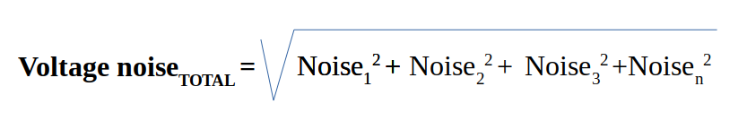
*I off course understand that noise of every stage must be calculated and eventually the total noise. Given the 1.26mV smallest signal that i have calculated, there will probably be lots of noise but i am not planning to go that low.

Can you pls help?

Regards

Manos Tsachalidis

  • Hi Manos
    I have notified the ADS4225 expert regarding your questions.
    He will provide a more detailed response soon.
    Best regards,
    Jim B
  • Hi Emmanouil,

    Sorry for the delay in reply.

    You should be able to DC-couple the LMH6881 output directly into the ADS4225 input by level shifting the LMH6881 supplies.

    For 0.95V ADC input CM, the LMH6881 supply can be set to +3.5V/-1.5V in-order to center the amplifier output CM with the ADC. The LMH6881 VCM will then need to be set to 0.475V for twice the gain from the amplifier VCM pin to it's output.

    Only caveat while level shifting the LMH6881 supplies is that the digital control for gain adjustment will need to reference with respect to the negative supply of -1.5V. If you decide to go this route, we should be able to recommend an appropriate level translator for the digital logic control.

    I think noise could be a concern while cascading multiple stages, since the noise from the first stage is gained up by the total gain in the signal chain in-addition to the noise contribution from the later stages. In-order to improve noise performance after the OPA659 FET input stage, you need to set most gain in the stage right after the OPA659 which will limit the noise contribution from subsequent stages. So, setting the 1st LMH6881 to 26dB max gain and then the 2nd LMH6881 to 10dB or lower gain would be desired in-terms of limiting the noise contribution from the front-end at the ADC.

    If you would like to set all the gain using a single device right after the OPA659, then the LMH6518 is an option too.

    Please let me know if this provides some visibility into the signal chain.

    Best Regards,
    Rohit
  • Thanks Rohit for your message,

    It is more or less clear to me what the common mode voltage options are.

    Regarding the noise however, it is not looking good.

    Is the thermal noise of the resistors being used in the LMH6881/2 included in the noise spectral density values? Should i be worried about those?

    Since we are talking about 50 or 100 Ohms opamp input/outputs i guess that the gain & feedback resistors will be of low value which in conjuction with the current noise would not be a huge additional noise.

    I am hypothetically calculating in an excel sheet multiple stages of opamps in order to be able to both have a high bandwidth with a tolerable noise level.

    Boosting up the gain with one single or two stages messes up the bandwidth so i have to make comprimizes here. What is the usual practice of opamps inside a low noise front end? How many are used?

    Also, i am having difficulty calculating the total amount of RMS noise that will be presented before the ADC's input (after the RC filter). I do undestand how noise is calculated for a single opamp stage but when it comes to multiple stages i get a bit confused. Let me be more specific so that you can undestand my concerns:

    Gains are #1=0dB, #2=26dB, #3=14dB & #4=6dB (Total gain= 26+14+6=46dB)

    BW (gain 0dB) are #1=1GHz, #2=2.4GHz, #3=2.4GHz & #4=1.8GHz

    BW (gain as per app) are #1=1GHz, #2=120MHz, #3=479MHz & #4=900MHz

    RC BW -3dB = 120MHz

    Example: opamp with BW 100MHz and gain 0dB.

    *For simplicity purposes let's assume that voltage noise density mentioned below already includes Current noise (converted to voltage noise), Resistors thermal noise (if any) and 1/f noise.

    If the voltage noise density of an opamp (always refering to its' input) is 5nV/√Hz then the output noise is: 5nV * √100MHz * Gain(1x) = 50μV RMS

    Now if the gain is 20dB (10x) then the BW gets devided by 10 and is now 10MHz, so the output noise is now: 5nV * √10MHz * Gain(10x) = 158μV RMS

    My question is: What will be the noise at the output of the RC filter?

    I am thinking... I should calculate the total bandwidth of all opamps 1,2,3,4 & RC combined and then multiply the input noise of opamp #1 with the square root of the combined bandwidth of all opamps & rc filter.

    Then, calculate the input noise of the opamps #2 and multiply with the square root of the bandwidth of opamps 2,3,4 & RC combined. Then do the same for opamp #3 & #4.

    Eventually combine all voltage noise values based on the foormula:

    Can you pls confirm whether my thinking is right?

    As far as i know the calculation of multiple opamps' bandwidth is given by this formula:

    Every bandwidth value in the formula above must be first recalculated to the correct bandwidth if the gain is greater than 1 based on the GBP (Gain * BW = GBP)

    Bandwidth (gain: 0dB) = 1GHz, Bandwidth (gain: 20dB) = 100MHz. 100MHz is therefore the correct bw value to be used for an opamp with bw=1GHz @ gain: 0dB

    What about the RC filter bandwidth? How does that affect the overall bandwidth? It is 1 pole filter and it is therefore just like an opamp's gain roll off 20dB/decade.

    Would the above formula, that calculates total bandwidth, be right if the RC bandwidth were calculated along side the opamp bandwidths? Any suggestions on that?

    Since i am only considering TI components in this project i am hoping that you will provide some extra help.

    Can you pls confirm?

    Best regards

    Emmanouil Tsachalidis

  • Hi Emmanouil,

    You should be able to calculate the total cascaded noise contribution of the signal chain as follows:

    Vout_noise(tot)^2  = [(Vin_noise1*Av1)^2 + Vin_noise2^2]*(Av2^2) + ...

    where,

    Vout_noise(tot) = total output referred rms noise of the signal chain in nV/rtHz

    Vin_noise1 = input referred rms noise of the 1st stage in nV/rtHz

    Av1 = voltage gain of the first stage in (V/V)

    Vin_noise2 = input referred rms noise of the 2nd stage in nV/rtHz

    Av2 = voltage gain of the second stage in (V/V)

    So, if you know the input referred voltage noise of each stage, then the cascaded noise of two stages is the output referred noise of the first stage (Vin_noise1*Av1)^2 added in rms fashion with the input referred noise of the second stage (Vin_noise^2). This can be repeated for subsequent stages until you reach the ADC front-end.

    Remember that the Vout_noise(tot)^2 has units of V^2/Hz which is essentially noise spectral density. So, if you want to convert into voltage noise for the noise power BW of 120MHz, you will have to take square root of the Vout_noise(tot) and multiply the result with sqrt(BW).

    In-theory, the total noise contribution due to the front-end becomes = sqrt( Vout_noise(tot)^2 x BW). in Vrms

    I have attached an excel spreadsheet that will allow you to calculate the total noise contribution for your front-end. The calculated total noise contribution due to the analog front-end is ~ 300 uVrms.

    NoiseAnalysis_OPA659+LMH6881_031419.xlsx

    Please let me know if there are questions.

    Best Regards,

    Rohit

  • Hi Rohit,

    I am really grateful for your time.

    The excel sheet that you put together was a great help.

    I have been watching the TI videos about opamp noise but also read quite a few app notes that i found on the internet.

    I haven't been using the NF in my calculations. Despite that, i calculated the total noise based on the first two stages as they were dominant and the result was the same.

    An insignificant difference was there but it is just of no importance. See the attached excel.

    Attached: TI_NoiseAnalysis_OPA659+LMH6881_031419.xlsx

    The resulting SNR of the ADC is a mess as you probably saw and is unacceptable for a 12bit dso. Replacing the OPA659 with the OPA859 and LMH6881 with LMH6518 resulted in a visible improvement but even that is not good.

    That off course occurs only at low voltage scales where the front end gain is high but that destroys the ability of the adc to distinguish between low level signals and noise.

    I was hoping to go down to 1mV / Div but given the resulting noise even with OPA859 & LMH6518 i do not see how that is possible.

    After improving the noise performance by replacing the opamp candidates, SNR was 41dB @ 46dB gain not including the thermal noise of the high vltage input attenuator.

    Is that supposed to be normal? I mean, what is the SNR of a good oscilloscope when its' front end is set to its' highest gain?

    Is there anything else i can do to improve the noise performance?

    Best regards

    Manos

  • Hello Emmanouil,

    What I recommend you do instead of trying to do the noise calculation in excel is try to recreate your circuit design in TINA-TI with all those components. Doing this will allow you to not only clearly do noise and gain calculations but also immediately adjust and change components to see their impact. Improving noise is a complicated and tricky task but is completely detailed in our precision amps videos that you have been watching.

    Here is a video on doing noise analysis with an FDA.
    training.ti.com/ti-precision-labs-op-amps-fully-differential-amplifiers-noise-analysis-advanced-compensation

    The TINA files for each of the components you have mentioned are under the tools & software folder of each product. You can recreate your circuit in TINA, then follow the TI precision labs videos to calculate noise and output. Once you do that, you will also have a better understanding on what specifics you are looking for in terms of parts. Once you recreate your circuit in TINA, go ahead and post it on here so I can also play around with it to see if I can help.

    Thanks!
    -Karan
  • I would like to sincerely thank all of you for your suggestions and time you took to post your responses.

    Best Regards

    Manos Tsachalidis