This thread has been locked.

If you have a related question, please click the "Ask a related question" button in the top right corner. The newly created question will be automatically linked to this question.

TINA/Spice/ADC12DL3200: SYSREF processing activity

Part Number: ADC12DL3200
Other Parts Discussed in Thread: TINA-TI, , LMX2594

Tool/software: TINA-TI or Spice Models

Hi,

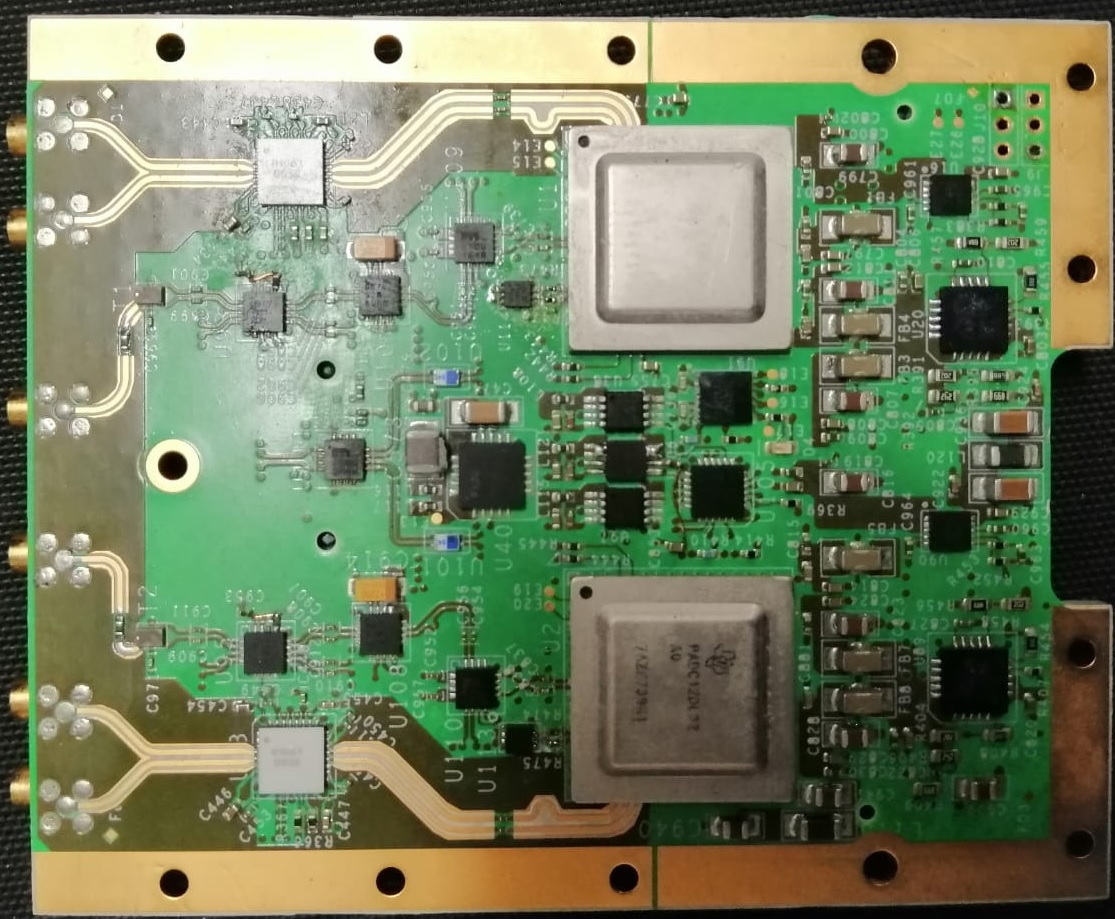
I'm design a board with four ADC12DL3200 and now I'm trying to sync the ADCs.

I've enabled the SYSREF receiving setting
- SYSREF_RECV_EN = 1
- SYSREF_PROC_EN = 1
- SYSREF_LVPECL_EN = 1.

I've send SYSREF signals to the ADCs and I've verified that the bits 
ALIGNED =1 
REALIGNED = 1.

Then I've measured the data phase match and change the phase of a specific SYSREF signal.

I've resetted the ALIGNED and REALINGNED bits and send several SYSREF signals.

After this I've verified that the ALIGNED = 1 but REALIGNED = 0!

Why the SYSREF signals are received but not processed? 

Is there a specific comand to able the processing?

i'm looking forward to hearing from you

Regards.

Daniele Sassaroli

  • Hey Daniele,

    I forwarded your question to a device expert. They will be with you shortly.

    Thanks

    Yusuf
  • Hi Daniele
    Are you generating the SYSREF signal so that it is synchronous to the ADC Clock signal and is a subharmonic of that signal?
    See section 7.3.4 of the ADC12DL3200 datasheet.
    If the SYSREF frequency is correct according to the equation in that section then repeated captures of SYSREF will only result in the ALIGNED status bit being set. This indicates that SYSREF was captured, but the phase was such that the internal clocks did not need to be re-aligned.
    The REALIGNED status bit will only be set if the received SYSREF signal causes the internal clock phases to be re-aligned to a new phase. If the internal clocks stay at the same phase the REALIGNED bit is not set.
    I hope this is helpful.
    Best regards,
    Jim B
  • Hi Jim,
    thanks for your analysis.

    In our project we don't use a repetitive SYSREF but only single pulses to
    calibrate the SYSREF window and to alignment the Strobe signals.

    In this case, we've verified that the ALIGNED status works correctly while
    the REALIGNED bit no: there are condition where the REALIGNED bit is 1
    and condition where this bit is 0.

    Is there a way to force the REALIGNED activity?


    Thanks in advance.


    Best Regards,
    Daniele
  • Hi Daniele
    Are your SYSREF pulses generated such that they are synchronous to the ADC CLK?
    Are the SYSREF pulses created with some frequency relationship to CLK such that future SYSREF pulses will only occur at specific times?
    Or is the timing of future SYSREF pulses random in relationship to previous pulses or ADC CLK?
    Best regards,
    Jim B
  • Hi Jim,
    the SYSREF is generated synchronous with the ADC_CLK (use the same base clock to generate ADC_CLK and the SYSREF).
    The SYSREF pulse is not short but it remains high for 64 ADC_CLK cycles. Each time that I generate a SYSREF pulse, I also verified that there is a window in the SYSREF_POS registers (2E-2D-2C).
    Best Regards,
    Daniele
  • Thanks Daniele
    Is there any specific timing relationship between the rising edge of a previous SYSREF pulse, and those that are generated in the future?
    Can the relative timing be variable by a single ADC input CLK period, or is there a larger integer number of CLK periods that determines the spacing.
    Also, what settings are you using for LDEMUX and LFRAME?
    Regards,
    Jim B
  • Hi Jim,
    I'm using a 31.25 MHz TCXO to generate the 2 GHz clock (using a PLL LMX2594) and to resample the SYSREF
    signal generated by a FPGA. The SYSREF signals are generated always synchronous with the 31.25 MHz and the ADC_CLK. The distance between two SYSREF signals are not constant but a multiple of 31.25 MHz.
    The LDEMUX = 1 and LFRAME = 8.

    Regards,
    Daniele
  • Hi Daniele
    According to the equation in the datasheet and your clock frequency and register settings, the maximum SYSREF frequency would be 125 MHz.
    The SYSREF pulse you apply is synchronous to 31.25 MHz, which is 1/4 of 125 MHz.
    The first SYSREF pulse that is applied to the ADC will realign the internal clock phase to match that of the SYSREF. In most cases the REALIGNED bit will be set after the first SYSREF pulse is captured. The only reason it would not be set is if the internal clock phase had happened to be at the proper alignment already.
    Subsequent SYSREF pulses synchronous to 31.25 MHz will occur at the proper alignment, so the internal clock phase doesn't need to be realigned. That is why the REALIGNED bit is not set for these additional SYSREF events.
    I hope this is helpful.
    Best regards,
    Jim B
  • Hi Jim,
    I'm agree with you, because I've observed that the delta phase between the two channels is constant.
    The problem is that this delta phase in not good for the system and I've tried to modify
    the SYSREF delay externaly to the ADC (using the internal TAP of the FPGA) of one or two ADC_CLK cycles.

    Changing the SYSREF position, I'll suppose that the SYSREF position change and the ALIGNED = 1 and REALIGNED = 1 . Instead the ALIGNED = 1 (first I had resetted), the REALIGNED = 0 and the delta phase is the same.

    Do you think that the ADC sees the same SYSREF?

    Thanks in advance.

    Best Regards,
    Daniele
  • Hi Daniele

    You say that you are seeing a constant phase delta between the different ADCs on the board, but that the delta phase is not good for your system.

    Are the CLK signals delivered to the 4 ADCs routed with matched delays so they are all phase aligned?

    How much phase delta are you seeing (comparing the same DxCLK or DxSTR signals on each of the 4 ADCs)? Even if the input CLK signals are phase aligned there will be some differences due to part to part variation in Tod (output delay) between the 4 ADCs.

    Best regards,
    Jim B
  • Hi Jim,

    The clocks are distributed using several buffers and switchs and this network has a delay that is not easy to manage. This is one of the reasons to manage the delay of the SYSREF signals.

    The CLK and input signals are routed with matched traces and simulated using CST Microwave SW.

    Moreover the ADCs uses different inputs: 2 ADC use INA inputs and and 2 ADC use INB inputs. In particular, if the board distributes the same input signal, clock and SYSREF at two different ADCs (LDEMUX = 1 and LFRAME = 8) and one ADC uses INA input and the other ADC uses INB input, Is there a specific difference between the phase of input signals acquired?

    Today I will do others measurement to study the results and maybe I understand the problems.

    Regards,
    Daniele
  • Hi Jim,
    The clock distribution network is composed of buffers and switchs and it is not easy to calculate the complete delay or mismatch between each clock route. However the clock traces routed are matched and simulated with CST Microwave Studio.

    The delta phase observed is about 1/2/3 samples and I don't think it is only related to part variation in Tod between the four ADC.

    I've also the following questions:

    1. I've instantied two couples of ADCs. In each couple of ADC, one ADC1 uses INA such as RF input signal (the INB is terminated) and the other ADC2 uses INB such as input signal (the INA is terminated). Both ADCs works in DES-MODE (LDEMUX = 1 and LFRAME = 8). If the clock and SYSREF traces are perfectly traced, the difference in the ADC input (INA for ADC1 and INB for ADC2) maybe produces a mismatch in the sample of the ADCs. What do you think?

    2. In the board, I can move the SYSREF signal respect the clock signal phase for 1/2 ADC clock cycles. When I move the SYSREF for a little quantity, I observe ALIGNED = 1 and REALIGNED = 0. The ADC doesn't recognize the timing change of the STROBE signal. Is there a minimum quantity of time to move the SYSREF signal that the ADC recognizes and then changes the STROBE timing? What the minimum change of STROBE timing?


    Regards,
    Daniele
  • Hi Daniele
    There can be some difference in the aperture delay (See tAD in Table 6.10) between the converters. Even if the input clocks are exactly aligned the variations in aperture delay will make the apparent sample instant appear earlier or later even if the exact same input signal is present at all ADCs. You should be able to adjust the ADC aperture delay setting to compensate for the variation as long as a known input signal is present. I would expect the variation is less than one ADC clock period. The typical tAD value is listed as 360 ps, and the part to part variation will be some fraction of this amount.
    The REALIGNED bit should be set when SYSREF is moved 1 or more ADC CLK periods earlier or later as compared to when SYSREF was originally captured.
    The output timing shown in Figures 1-7 illustrate the time from SYSREF captured by the rising edge of CLK to the resulting output signal timing in particular tLAT(STB). If SYSREF is captured one CLK edge earlier or later, all of the output signals should shift earlier or later by the same amount.
    Best regards,
    Jim B
  • Hi Jim,

    thanks for your details.

    I've prepared two documents:

    - the first document is a descriprion of the board and the method used to sync the data;
    - the second document is the list of the command used to configure the ADC at the power on.

    I've problems to understand the way to attach these file. Can you help me?

    Thanks in advance.

    Best Regards.

    Daniele

  • Hi Jim, I've discovered another misunderstanding. Reading the datasheet, I've saw that in my ADC configuration

    the data sample are aligned following A,C,B,D buses and not A,B,C,D: see the figure 7. Is it correct?

    Best Regards,
    Daniele

  • Hi Jim,

    do you have any news for the last two messages?

    I'm looking forward to hearing from you.

    Regards,
    Daniele

  • Hi Daniele
    You can attach your files by first clicking the "Insert Code, Attach Files and more..." link below the reply window, and then using the file attach (paper clip) icon above the more advanced reply window.
    I am confirming the proper data base sample order and hope to have that information tomorrow.
    Best regards,
    Jim B
  • Hi Jim,
    in the attached file you can find a description of my design and the file that I use
    to configure the ADC.
    Can you check if the configuration is correct?
    Can you check if the ADC_CLK and SYS_REF ADC signals are correctly driven in my design?

    I'm looking forward to hearing from you.
    Regards,
    Daniele
  • Hi Daniele
    I will review the files you have attached.
    Regarding Figure 7 in the datasheet, there is an error.
    The samples are actually ordered as A, B, C, D, not A, C, B, D as shown in the figure.
    The datasheet will be updated to correct Figure 7.
    Best regards,
    Jim B
  • Hi Jim,

    ok for the Figure 7.

    Do you have any news for the files attached?

    I'm looking forward to hearing from you.

    Best Regards,
    Daniele

  • Hi Daniele
    Sorry for the delay. I should have some feedback on your current setup details tomorrow.
    Best regards,
    Jim B
  • Hi Daniele

    I reviewed your settings and the additional information regarding your system and have a few questions:

    • When you "send a SYS_REF signal and Verify the SYS_REF eye" how many times does SYSREF toggle from low to high? If it is only 1 time currently, try sending it 3 times in succession (or more) and then reading the SYSREF_POS register. That should give the most consistent results.
    • When you adjust the SYS_REF delay for one of the ADCs, what is the timing step of the TAP adjustment?
    • Can you confirm the ADC1_CLK_P/ADC1_CLK_N (and similar clock signals for ADC2) are AC-coupled to the ADC clock inputs to allow the proper common mode voltage at the CLK inputs?
    • Can you check the common mode of the SYS+/SYS- signals applied to the ADCs? I know you are using the SY89327 ECL driver and the DC-coupled LVPECL SYSREF termination mode. I just want to see what voltage that gives at the ADC SYSREF inputs?
    • In your register settings file, you said the values written to register 029 are first 2 and then 6. Did you mean to say 0x20h and 0x60h? These are the correct values. Writing 2d and 6d (0x02h and 0x06h) would not give the expected results.

    I hope this is helpful.

    Best regards,

    Jim B

  • Hi Daniele
    Do you have any updates regarding my questions above?
    Has this issue been resolved?
    Best regards,
    Jim B
  • Hi Jim,

    I'm not resolved the issue. Below  there are your questions and my answers

    • When you "send a SYS_REF signal and Verify the SYS_REF eye" how many times does SYSREF toggle from low to high? If it is only 1 time currently, try sending it 3 times in succession (or more) and then reading the SYSREF_POS register. That should give the most consistent results. I usually send not a single impulse but a signal that is normaly low and when high, it's high for 16 or 32 clock cycles. 
    • When you adjust the SYS_REF delay for one of the ADCs, what is the timing step of the TAP adjustment? The TAP time step is about 5 ps.
    • Can you confirm the ADC1_CLK_P/ADC1_CLK_N (and similar clock signals for ADC2) are AC-coupled to the ADC clock inputs to allow the proper common mode voltage at the CLK inputs? Yes it is.
    • Can you check the common mode of the SYS+/SYS- signals applied to the ADCs? I know you are using the SY89327 ECL driver and the DC-coupled LVPECL SYSREF termination mode. I just want to see what voltage that gives at the ADC SYSREF inputs? I will try in the next days.
    • In your register settings file, you said the values written to register 029 are first 2 and then 6. Did you mean to say 0x20h and 0x60h? These are the correct values. Writing 2d and 6d (0x02h and 0x06h) would not give the expected results. I write 0x20 and then 0x60 at the start up. Then, when I must write the new delay value I write directly 6XHex where X is the delay measured through the SYSREF_POS registers.

    Now I'm working at 4 GHz clock and I've problems to center the SYSREF Windows:

    1. I send 10 SYSREF signals (high for 32 clock cycles) and read the three registers SYSREF POS. In this situation, I've observed, in the SYSREF_POS windows, windows of 7 bits (1000001) that is about 500 ps = clock period of 2 GHZz. Then I select the value that I must write in the four 29 registers and I write their values in these registers. When I send another 10 SYSREF signals the SYSREF_POS Windows shift of 1/2 or 3 bits and I must change another time the value in the 29 registers. Why? This process is potentially really heavy. Is it correct?

    2. I the SYSREF_POS I've 2/3 complete Windows and four each ADC I can set different values in function of the Windows read. Is the window selected  change for an ADC, I may observe a change in the data allignment of the four ADCs? 

    I look forward to hearing from you.

    Regards,
    Daniele 

  • Hi Daniele
    Sorry for the delay. I'm reviewing this information now and will respond tomorrow.
    Jim B
  • Daniele,

    I am the lead digital designer for the ADC12DL3200, and I'd like to help resolve your question.

    I'm curious about the exact order of your steps.

    The REALIGNED bit will not go high unless you clear it BEFORE you apply a shifted SYSREF pulse. If you apply the shifted SYSREF pulse first and then clear REALIGNED, then you will not see REALIGNED=1.

    The REALIGNED bit simply goes high if a SYSREF pulse is processed, but it is inconsistent with the previous SYSREF pulse (e.g. the number of ADC clock cycles between the two pulses is not a whole number of LVDS frame periods).

    The ALIGNED bit goes high whenever any SYSREF pulse is processed, regardless of whether it is consistent with the previous pulse. It is intended as a confirmation that SYSREF did in fact get received by the ADC.

    Double check that your shifted SYSREF pulse is actually shifted enough to trigger a re-alignment (shifting it less than one ADC cycle may not cause any re-alignment).

    Also make sure you keep LVDS_EN=1 during your testing. If you program LVDS_EN=0, the internal frame counter is reset and requires a new SYSREF pulse to re-establish its phase with respect to SYSREF.

    Let me know how I can help further.

  • Daniele,

    In regard to this question:

    1. I send 10 SYSREF signals (high for 32 clock cycles) and read the three registers SYSREF POS. In this situation, I've observed, in the SYSREF_POS windows, windows of 7 bits (1000001) that is about 500 ps = clock period of 2 GHZz. Then I select the value that I must write in the four 29 registers and I write their values in these registers. When I send another 10 SYSREF signals the SYSREF_POS Windows shift of 1/2 or 3 bits and I must change another time the value in the 29 registers. Why? This process is potentially really heavy. Is it correct?

    Changing SYSREF_SEL shouldn't impact the SYSREF_POS result. I've seen a similar problem where the SYSREF input could shift by about half an ADC clock cycle and it was caused by a bench setup that generated SYSREF through a synthesizer (it was probably multiplying the ADC clock frequency up and then dividing it down without keeping the divider aligned with the original ADC clock). It would "randomly" shift the SYSREF by half an ADC cycle when disabling and re-enabling the synthesizer (based on when the divider was reset with respect to the ADC clock). Review how your FPGA actually creates SYSREF from the ADC/PLL clock (review all PLLs and frequency dividers to make sure they all have deterministic latency).

    Try your experiement again, but don't change SYSREF_SEL. Just input some SYSREF pulses, check SYSREF_POS, and then input some more SYSREF pulses and check SYSREF_POS again.

    Since you are generating SYSREF from an FPGA, you will probably have a hard time meeting setup and hold timing on SYSREF (vs. ADC clock) over process/temperature/supply voltage. You will probably need a calibration algorithm like you are currently running (adjusting SYSREF delay until you can confirm all ADC channels are aligned). However, each time you add delay to SYSREF in the FPGA, you are re-evaluating SYSREF_POS and set SYSREF_SEL. This is problematic. This might be canceling out your FPGA delay changes because SYSREF_SEL controls an internal SYSREF delay inside the ADC. Pay close attention to how your computed SYSREF_SEL value trends up or down as you gradually increase the FPGA delay.

    If you want to delay SYSREF by one ADC clock cycle, program SYSREF_SEL to a larger value that is centered into the second SYSREF_POS window (instead of the first window).
  • Hi Paul,

    thanks for your analysis and suggestions.

    First of all, I've measured the SYSREF signal levels and I've observed these levels:

    - High = 1.4V;

    - Low = 0.9V.

    Considering that the SYSREF input is in DC mode (SYSREF_LVPECL_EN=1) , are these levels correct or not?

    Second, I don't understand the following phrase:

    Try your experiement again, but don't change SYSREF_SEL. Just input some SYSREF pulses, check SYSREF_POS, and then input some more SYSREF pulses and check SYSREF_POS again.

    You say that the SYSREF_POS mustn't be change from SYSREF_SEL selection or SYSREF pulses, is it correct?

    When the SYSREF is processed (REALIGNED = 1), have the SYSREF_POS registers the same old values?

    Usually, LVDS_EN is 1 during the tests.

    The SYSREF signal is generated using the REFCLK signal = 31.25 MHz. This REFCLK is also used to generate the 2 GHz ADC clk with a LMX2594 by TI.

    The ADC clk and the REFCLK signals have the same phase and consequently the SYSREF signal has the same phase of the ADC clk.

    I look forward to hearing from you.

    Regards,
    Daniele 

  • I'll double check with the analog design team on the LVPECL voltage levels.

    I'll try to restate myself.  The SYSREF_SEL value you write should not influence the SYSREF_POS result you read back. However, something else might be influencing SYSREF_POS.

    You said you were observing a change on the SYSREF_POS result after changing SYSREF_SEL. I was trying to propose an experiment to see if your observed change would still occur even if you didn't modify SYSREF_SEL.

    SYSREF_POS and REALIGNED are  independent status values.  SYSREF_POS is just telling you about the arrival time of SYSREF with respect to the DEVCLK waveform.  It provides very fine-grained phase information.

    REALIGNED is telling you if a SYSREF pulse actually caused the internal frame counter to realign. This occurs if the SYSREF edge is sampled high on the wrong DEVCLK cycle compared to the previous SYSREF edge.

    I recommend always reading REALIGNED first, and then only clear it if it returned a 1. This way you never miss any re-alignment events. If you just unconditionally clear it, you could be missing an event.  If you clear REALIGNED, it won't set itself again until you modify SYSREF enough to cause the frame counter to readjust again.

    It's possible for SYSREF_POS to change and REALIGNED to stay at 0. It's also possible for REALIGNED to be set, even while SYSREF_POS doesn't change.  It all depends on how much the SYSREF phase changes.

    Small phase changes on SYSREF that are within the setup/hold window with respect to DEVCLK will be reflected on the SYSREF_POS result, but will not cause REALIGNED to fire.

    Large phase changes on SYSREF that cause it to be sampled by a different DEVCLK cycle (as compared to previous SYSREF pulses) will be reflected by REALIGNED. SYSREF_POS will also reflect the change if it is not a whole number of DEVCLK cycles.

    As for the LMX2594, I'm not sure the 2GHz output is deterministically aligned to the 31.25MHz REFCLK input (it might change when the LMX2594 is power cycled or reconfigured).  I suspect this because it has a channel divider to produce the 2GHz output from the VCO. I don't know if there is anything to ensure that the channel divider output is aligned with the reference clock input. I'm not very knowledgeable about the LMX2594. For example, if the channel divider is 5, there may be 5 possible phase differences that can occur between the 2GHz output and the 31.25MHz input.

  • I checked the voltage levels with the analog team that designed the SYSREF receiver logic. Here is the response:

    If I understood well, LVPECL driver is DC coupled to the SYSREF receiver, which has 2x single ended 50 Ohm termination towards GND.

    The SYSREF receiver can handle the aforementioned input levels (VIH=1.4V and VIL=0.9V). However, these conditions put the operation of the block above the designed EM limits for 15%. EM wise (which was a challenge) it was designed for slightly lower input common mode.

    I hope this helps.

  • Hi Daniele
    Have you made any progress on this?
    Do you have any updated information related to the experiments that Paul asked about?
    Best regards,
    Jim B
  • Hi Jim,

    in the last two weeks I had problems to do the test.

    I think that the next week I will have the time to close the test of RF section and in particular the
    experiment suggested by Paul.

    I have attached a picture of the RF section of the board under test. You can see only two ADCs and the T&H.

    Thank for your support.

    Best Regards,
    Daniele

  • Hi Daniele

    Please let us know when you have updated information to discuss or if you resolve this issue.

    Best regards,

    Jim B