Other Parts Discussed in Thread: TIDA-01214, ADS8688, DAC7571
Hi
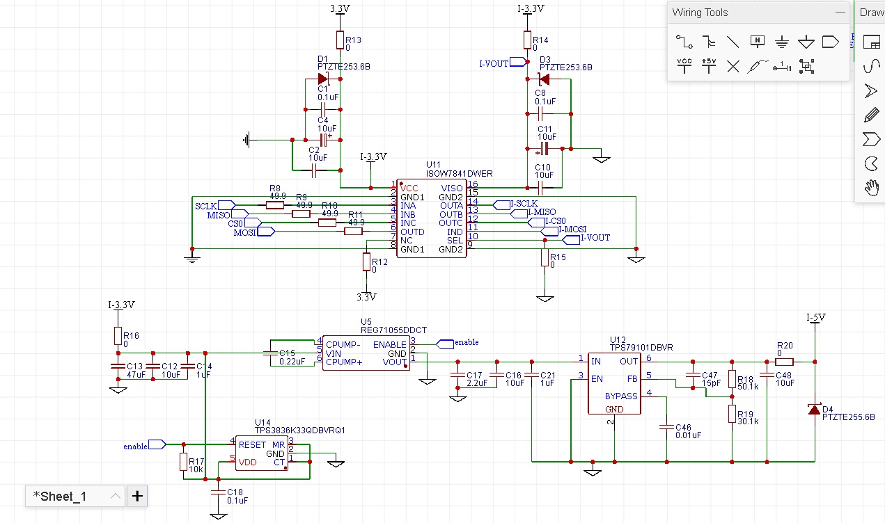
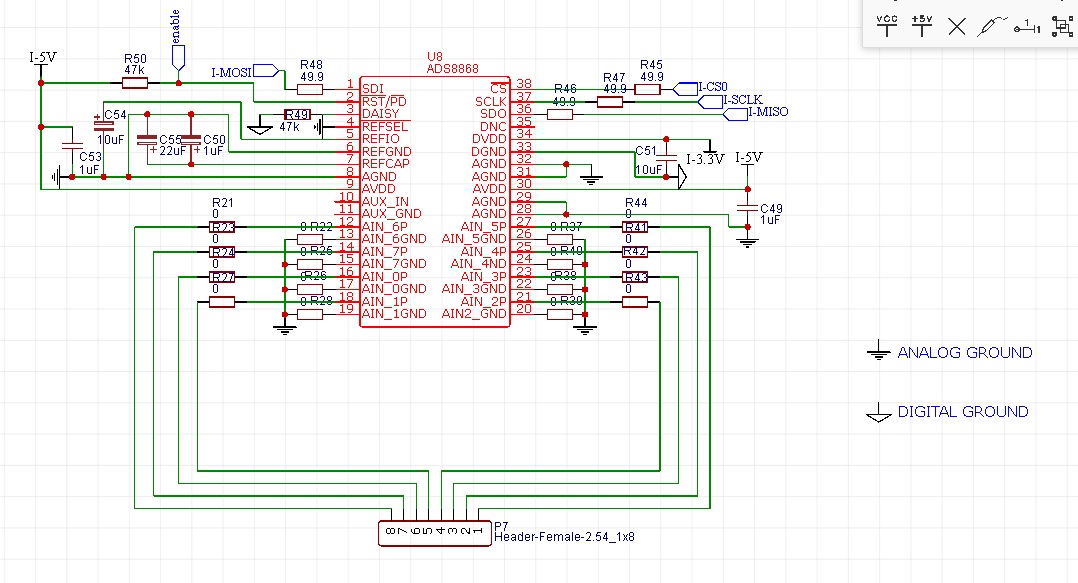
I would like to ask if the setup in the picture could be taken into account for the setup of ads8668 controlled by a teensy 3.6
Kind regards
Original question:

Hi
I would like to ask if the setup in the picture could be taken into account for the setup of ads8668 controlled by a teensy 3.6
Kind regards