This thread has been locked.

If you have a related question, please click the "Ask a related question" button in the top right corner. The newly created question will be automatically linked to this question.

TINA/Spice/ADS1115: Data converters forum

Part Number: ADS1115
Other Parts Discussed in Thread: TINA-TI, , ADS1120, ADS112C04

Tool/software: TINA-TI or Spice Models

Dear data converter engineer,

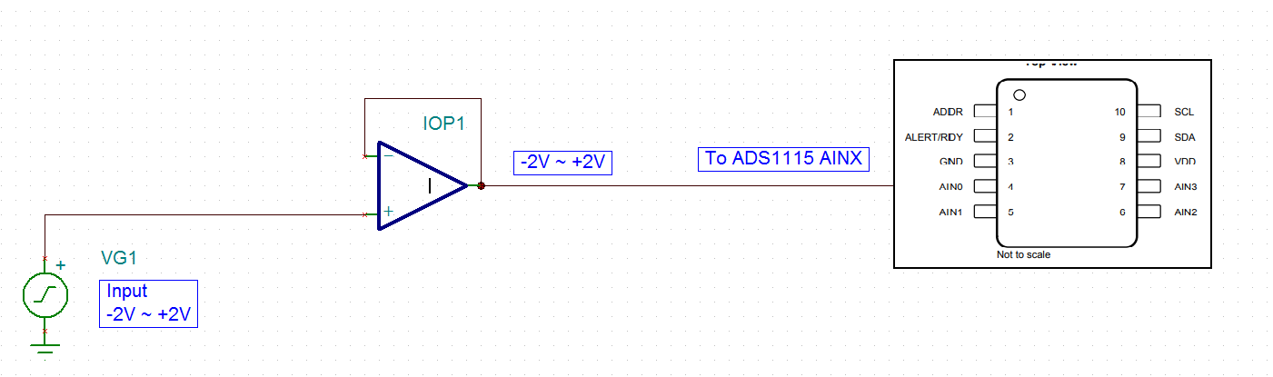
Hi, I am an engineer who needs to develop negative to positive voltage sensing mechanism.

So I want to know whether i can use ADS1115 to measure negative voltage or not.

If so, how should i set the circuit or register?

My expected circuit is shown below.

I am looking forward to your solutions.

Thank you in advace.

  • Hi 'Univ Seoul',

    welcome to our e2e forum and thank you very much for your interest in our devices.

    The ADS1115 itself can unfortunately not measure signals below GND. The absolute voltages on every input have to be >=0V.
    The device can measure negative differential signals. What that means is, if you for example select AIN1 as the positive ADC input and AIN0 as the negative input, you could measure signals which are AIN1=1V and AIN0=3V. Differentially this is a negative signal VIN = V_AIN1 - V_AIN0 = 1V - 3V = -2V.
    So what you would have to do in order to use ADS1115 is to level shift the signal using the external amplifier to a common-mode voltage of 2.5V.
    You would connect one input (e.g. AIN0) of the ADC to 2.5V and another input (e.g. AIN1) to the output of the amplifier which does the level shifting.
    The absolute voltage on AIN1 would then swing between 0.5V and 4.5V. The differential voltage VIN = V_AIN1 - V_AIN0 would swing between -2V and +2V.

    Another option would be to use ADS1120 (SPI) or ADS112C04 (I2C) together with a bipolar analog supply, that is AVSS=-2.5V and AVDD=2.5V.
    In that case you would connect one input (e.g. AIN0) to GND = 0V and the another one (e.g. AIN1) directly to the VG1 signal. No external buffer would be required in that case because both the ADS1120 and ADS112C04 integrate a buffer.

    Regards,

  • Dear Joachim Würker,

    Thank you very much for your kind reply.

    By the way, I would like to know the reason why ADS1115 cannot measure negative voltage when it use as a single ended input system in contrast differencial ended system makes it.
    So may I know about PGA circuit diagram in block diagram in ADS1115?

    And secondly, I'd like to know about meaning of "full scale range" when we use it as a single ended input and differential ended input.
    If I chose single ended input such as AINP=AIN1, AINN=GND input system, what does +- 2.048V mean?? What voltage Can I measure?? "0V to 4.096V" and "0V to 2.048V"?

    Thank you very much in advance.
  • Dear 'Univ Seoul',

    the ability of the ADS1115, and of many of our other ADCs, to measure voltages below GND does not depend on if the configuration is single ended or differential. It depends on the specific ADC design.
    For the majority of our ADCs the absolute voltages at the inputs of the ADC have to stay within the limits of the provided analog supply. Means in order to measure voltages below GND you would need a bipolar analog supply. But not all our ADCs allow using a bipolar analog supply. You can usually determine that by looking at the Recommended Operating Conditions table in our datasheets.
    - The ADS1115 datasheet does for example specify that the absolute input voltage has to stay between GND and VDD.
    - In addition the power supply is limited to VDD = GND + 2V to GND + 5.5V.

    We have other ADCs designs as well that allow measurements below GND while using a unipolar external analog supply. However those designs do then either integrate a negative charge pump which creates a negative analog supply internally, or they integrate a difference amplifier input stage.

    When using a single-ended configuration with ADS1115, where AINN = GND and FSR = +/-2.048V, it means you can only measure voltages between AINP = 0V and +2.048V. The negative range of the FSR cannot be leveraged in that case.
    If you were to use a so-called pseudo-differential configuration where AINN = 2.5V, then you could leverage the complete FSR of +/-2.048V. Means AINP could then swing between 2.5V - 2.048V and 2.5V + 2.048V.

    Regards,