This thread has been locked.

If you have a related question, please click the "Ask a related question" button in the top right corner. The newly created question will be automatically linked to this question.

ADS131A04: ads131a04 analog input to digit output mapping curve

Part Number: ADS131A04

hi,

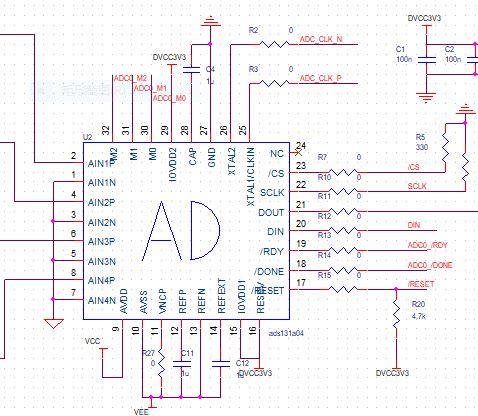
   I am using the ads131a04 to sample 4 channel analog signals. I have at least two problems reffering to the vref and digit outputs. I am using the internal refference voltage and Bipolar Analog Power Supply. the Negative Charge Pump is disabled. please see the attached schematic, where VCC is 2.7V and VEE is -2.7V.

1. REFP is not as expected. when I set it to 2.442V(or after powering up), What I get is about -1.3V; when I set it to 4.0V, What I get is about1.6V;

2. The digit output is hard to explain. When a DC voltage of about -0.5V is applied to the AIN?P, the output code is 0xED?? or 0xF0??. It seems like there is a big DC offset in the output code. I have failed to find how the output codes is related to the input voltage and the refference voltage, in the datasheet.

thank you!

  • seems like the digit output codes are right. However it is still not clear to me about the relationship between the voltage of REFP and the internal vref.
  • Feng,


    For the ADS131A04, the internal reference is generated from the analog portion of the supply. This means that the negative lead of the internal reference is connected to AVSS (in your schematic this is VEE). If your supply is ±2.7V as you mentioned in the first post, then AVDD=2.7V and AVSS=-2.7V.

    This would mean that when the internal reference is 4V, the output of REFP would be 1.3V with respect to the ground. If the internal reference is 2.442V, then the output of REFP would be -0.258V with respect to ground.

    You have already added this in your schematic, but you should make sure that C11 is installed. There should be a 1uF capacitor from VREFP to VREFN. VREFN should also be connected to AVSS.

    As for your other question, you've already figured out the output of the ADC is reported in two's complement notation. If you have a reference of 4V, and the input of the ADC is -0.5V, then the output of the ADC will be:

    (-0.5V*2^23)/4V = -1048576 = F00000h

    This is described in the 9.5.1.5 Data Words section of the datasheet on page 38.

    For your setup, go back and check the connection of REFP, REFN and AVSS. If the voltages are as I mentioned then we've figured this out. If not, then we can re-open this post and continue to debug the circuit.


    Joseph Wu