This thread has been locked.

If you have a related question, please click the "Ask a related question" button in the top right corner. The newly created question will be automatically linked to this question.

ADS7961: Input Clamping

Part Number: ADS7961

I refer to a post, where it was stated, that the internal ESD diodes clamp to (+VA) with a max. current of 10mA.

I just want to validated, that this also applies to the ground. I assume this, because the max. input current is also stated with a negative value.

The reason:

I measure an output voltage, which drives an inductive load. During freewheeling (with zener diode), the voltage can become negative and so the measured voltage.

Thanks

Sebastian

  • Hello,

    What are the characteristics of your Zener diode?
    I am assuming that it has a forward voltage drop is 0.7V and, say our internal ESD has a will start conducting at -0.3V
    this would then mean the current would instead go through the ADC instead of the diode as designed.
    Even if the max freewheeling current is less than 10mA, this would wear down the device.
    I suggest placing a resistor in between the Zener diode and the ADC input to limit the current and not damage the device.
    What is driving your input, can you add a current limit resistor?

    Regards
    Cynthia
  • Hello Cynthia,

    I have to admit, that I was not precice enough. I already plan to measure the Voltage via a Voltage divider (nominal its 24V). During Freewheeling the output voltage my drop to -20V.
    The divider would be high enough to limit the current to <10mA.

    I just wanted the confirmation, that the internal ESD diode also clamps to AGND and is capable of the 10mA.
    I know it from other Datasheets, that the Voltage given as Absolute Maximum can be exceeded, when the current is limited. This information is missing in the ADS7961 Datasheet.

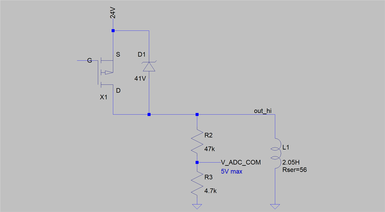
    Below i have an excerpt of my circuit for better understanding:
    Please note: due to Safety/System reasons I cannot put the Freewheeling diode in parallel to the load.

  • It is unfortunate that you cannot move the diode across the load, that would be best.

    With the fast switching of the FET there can be large spikes with currents above -10mA for a very short amount of time. If you can ensure that the current is kept with +/-10mA, then this should be fine.

    Have you considered adding a capacitor in parallel with R3? This would help with possible coupling on R2 during ON/OFF transitions, and overall help with noise

    Regards, Cynthia
  • Thank you,

    I have considered a Capacitor in parallel to R3, to reduce noise. But the value is not yet chosen.

    I Calculated the maximum negative voltage at Drain to: 24V-41V=-17V => rounded to -20V to regard Supply (24V) and breakdown (41V) variations.

    Via R2 this would result in a max possible current (the assumption when the ADC is not powered; which will not happen during FET switching): Imax=-20V/47kOhms=-425uA.
    This is more than Factor 10 away from the maximum limit of the internal ADC-ESD diodes.
    So I will have the value of R2 with a high enough value to limit the Current during the switching transients.

    Thank you for your replies.

    This resolved my issue.

    Sebasian