This thread has been locked.

If you have a related question, please click the "Ask a related question" button in the top right corner. The newly created question will be automatically linked to this question.

ADS1263: Data corrupted with external reference

Part Number: ADS1263

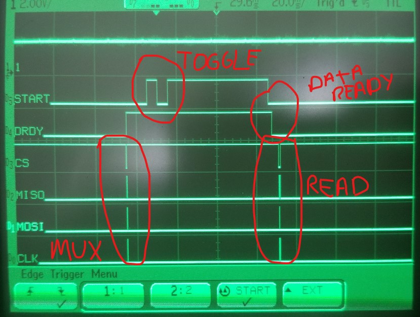
I am experimenting with a very interesting error of communication/acquisition with ADS1263.

Here is the setup:

- Using RPI to access the SPI

- Internal clock

- External reference voltage (2.048) connected AIN0-AIN1 (Single-ended - Neg Grounded)

- Scanning among across all AIN (DIFF) and VDig, Vana, TDAC and TEMP.

- Using serial command to start the acquisition

Everything is working fine, the data is clean, except the ADC1263 starts to reply data corrupted randomly after a few hours, sometimes a day. Interesting though, the same DOESN'T happen if I use the ADS1263 internal reference.  It seems the chip reset itself, or at least, the REFMUX switch to the internal reference (reading sometimes is compatible if I am using internal reference - not always).

I have implemented many different traps in my code and looks clean, it is working short term and long term with internal reference. Any clue where should I start to look?

thanks, --fernando

  • Hi Fernando,

    How do handling reading the data? Do you use an interrupt or poll for /DRDY to go low? Also, do you read data directly or issue an RDATA command before clocking out the data?

    Is possible that over time the SPI communication is not quite able to keep with the ADC's output data rate. If the MCU is not reading the data quickly enough, it might be clocking out data while a new conversion completes, in which case it's possible to get a combination of old and new data shifted out. The best ways to avoid this are:

    • Use a high priority interrupt to respond to the /DRDY falling edge and to retrieve the data quickly (well before the next /DRDY falling edge).
    • Using a faster SCLK (as fast as allowed) can help with clocking out the data faster.
    • Issuing the "RDATA" command before clocking out data will store the conversion data into a buffered shift register which will not get corrupted if a conversion completes while you're reading out the data. However, if you're not clocking out data fast enough eventually you will see a skipped channel.
    • Reducing the data rate to something that the MCU can keep up with can resolve the issue, AND I would recommend doing this while troubleshooting to see if this does help to resolve the problem!

    Regarding the reference voltage, I would make sure that your external reference voltage is buffered and stabled. Any changes in the reference voltage will get reflected in the ADC output codes. Do you have a schematic of your circuit that you could share?

    Are you seeing the RESET flag in the STATUS byte? If so that might indicate that a brown-out occurred and the device was reset.

  • /How do handling reading the data? Do you use an interrupt or poll for /DRDY to go low?/

    I poll the data for /DDY

    /Also, do you read data directly or issue an RDATA command before clocking out the data?/

    I am sending the RDATA cmd.

    /Is possible that over time the SPI communication is not quite able to keep with the ADC's output data rate. If the MCU is not reading the data quickly enough, it might be clocking out data while a new conversion completes, in which case it's possible to get a combination of old and new data shifted out./

    Could be! but why doesn't happen when I use the internal reference. The difference between working/not working is just the internal/external reference. I might be wrong, but this should create any extra delay or timing issues.

    The best ways to avoid this are:

    • Use a high priority interrupt to respond to the /DRDY falling edge and to retrieve the data quickly (well before the next /DRDY falling edge).
      • OK
    • Using a faster SCLK (as fast as allowed) can help with clocking out the data faster.
      • I have tried many different clk, and same result.
    • Issuing the "RDATA" command before clocking out data will store the conversion data into a buffered shift register which will not get corrupted if a conversion completes while you're reading out the data. However, if you're not clocking out data fast enough eventually you will see a skipped channel.
      • I may try to increase the clk, but again, doesn't explain why the circuit works with internal reference.
    • Reducing the data rate to something that the MCU can keep up with can resolve the issue, AND I would recommend doing this while troubleshooting to see if this does help to resolve the problem!

    I am using LTC6655 as the reference voltage (2.048V), unbuffered. I've checked the ref output when the problem happened and looks stable, no oscillation.

  • Hi Fernando,

    Do you have an example of the corrupted data that you can share to help me get a better idea of what you're observing?

    Probing the external reference voltage was a good idea. However, did you probe with a high-bandwidth oscilloscope or a low-bandwidth DMM? In the latter case you may see a stable DC voltage and not be able to obverse higher frequency oscillations.

    Also, I'm not fully understanding if the ADC is getting reset and reverting back to the internal reference. Your earlier comment hinted at a possible brown-out condition:

    Fernando Rafael said:
    It seems the chip reset itself, or at least, the REFMUX switch to the internal reference (reading sometimes is compatible if I am using internal reference - not always).

    Can you share the register settings that you observed before and after this reset, or perhaps the STATUS bytes that can be read out with the data to indicate if a reset has occurred?

    I'm afraid I need some additional details about the error(s) your observing to be helpful.

  • Chris,

    I made some SW/HW change to diagnose the problem.

    Here is more information:

    I probed the REF using oscilloscope and DVM, either is clean.

    The status bit is 0x40, means everything is working.

    I attached below the waveform using the START pin to initialize the acquisition.

    sequence:

    1) send the MUX_CH command

    2) toggle the START pin and start the conversion

    3) wait for DRDY signal (falling edge)

    4) read data ADC1 (0x12)

    First graphics, ADC working. Results match with the input. The top Trac is an analog signal (Ext REF)

    Waveform with problems:

  • here is the sequence of good and bad data received after a channel selection for the above waveforms.

    Working:

    Chip Select - 0 Serial Data - [70, 0, 69] -----> Select AIN4 and AIN5
    Chip Select - 0 Serial Data - [18, 0, 0, 0, 0, 0] ----> Read Data CMD
    --->>> Chip Select - 0 ADC Data Received - [72, 72, 117, 176, 223, 15] ------> Data received GOOD
    Read Status - 72 ----> Display the STATUS

    Not Working

    Chip Select - 0 Serial Data - [70, 0, 69] -----> Select AIN4 and AIN5
    Chip Select - 0 Serial Data - [18, 0, 0, 0, 0, 0] ----> Read Data CMD
    --->>> Chip Select - 0 ADC Data Received - [72, 73, 96, 124, 116, 128]------> Data received BAD
    Read Status - 72----> Display the STATUS (no change)

    REFERENCE 2.048 V

  • Hi Fernando,

    I'm sorry for the delayed response.

    The STATUS bytes you're showing (72 with good data, and 73 with bad data), indicate two different errors:

    1. STATUS = 72 = 0x48 (ADC1 data new & PGAL_ALM). You are reading a new conversion result, but the internal PGA is saturated, with at least one output signal that is trying to drive below AVSS+0.2V. Therefore, the result you're reading may appear to have a gain error since the PGA is operating in a non-linear region.
    2. STATUS = 73 = 0x49 (ADC1 data new & PGAL_ALM & RESET). In addition to the above information, the RESET alarm would seem to be indicating that the device got reset somehow. If this is not an SPI communication error, but the actual STATUS byte value, then its possible that you're reading the data from a different channel than what you're expecting.

      If you see the RESET bit set while reading data, I would recommend issuing commands to read back all of the ADS1263 registers and check to see how they are programmed, you may need re-program the device and restart the conversion on the last channel you were sampling.

      I would check to see if perhaps something in the code is accidentally toggling the nPWDN/nRESET pin or check the AVDD and DVDD supplies to make sure they are not seeing a brown-out condition. Perhaps adding larger decoupling capacitors to these supplies (near the ADC pins) may help to avoid this condition. Do you have a schematic of your circuit that includes how the ADS1263 is powered?

    On a side note, you can start ADC conversions by setting the START pin high. Toggling the START pin, as you are, might explain why sometimes /DRDY remains low after a conversion and other times it returns high. If you only want to perform a single conversion then I would set the START pin high, delay, then set START low and wait for the /DRDY signal to go low.