This thread has been locked.

If you have a related question, please click the "Ask a related question" button in the top right corner. The newly created question will be automatically linked to this question.

ADS1115-Q1: Voltage Reference value,

Part Number: ADS1115-Q1

Hi,

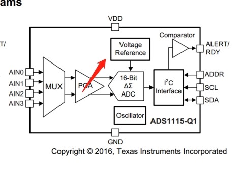
1.What is the Voltage Reference value of ADS1115-q1  ADC sample?There is no indication in the specification ;

2.What is the logical relationship between Voltage Reference and FSR?

Thanks!

  • Hi Neal,

    the ADS1115-Q1 has a very unique voltage reference implementation. You cannot really define what this reference voltage value is.
    You could arbitrarily say the reference voltage is 1.024V and then say the PGA offers a gain of 1 for the +/-1.024V FSR setting and a gain of 4 for the +/-0.256V FSR setting.

    The only thing that is important in the end is how to convert the conversion result into a voltage. For that you only need to know the FSR setting.
    The relationship between differential input voltage (VIN) and conversion result (Code) reads:

    Code / 2^16 = VIN / FSR

    Let's say you use a FSR = +/-0.256V as in your other post and the decimal output code of the ADC would read 100dec.
    That would mean the differential input signal applied to the ADC is:

    VIN = 100 / 2^16 x (2 x 0.256V) = 0.78125mV

    Regards,