This thread has been locked.

If you have a related question, please click the "Ask a related question" button in the top right corner. The newly created question will be automatically linked to this question.

ADS8881: Purpose of AVDD

Part Number: ADS8881

Hello,

I would like you to confirm about below.

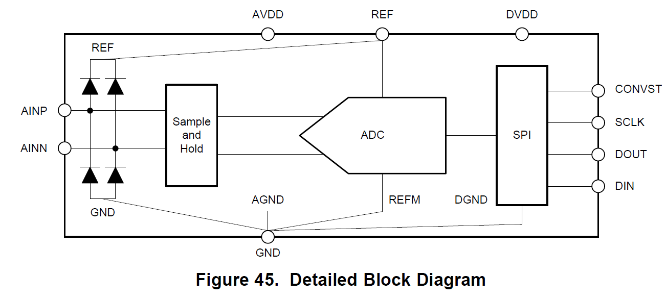
* There are two analog power (AVDD and REF) in ADS8881.

According to datasheet of ADS8881(Figure 45. Detailed Block Diagram), it seems that "REF" voltage is used for all of analog power source (supply for ADC, clamp voltage of input line).

According to datasheet, "The internal circuits of the device operate on AVDD" is described. So, this voltage is used for something. However, I'm not sure which purpose this supply is used.

So, could you please tell us internal usecase of this voltage ?

(Especailly, I would like to know when AVDD become low voltage than min spec of datasheet, which function will be affected.

One of function, I guess that this voltage is used for POR(Power on reset). so I can see that device will not boot up as one of issue..)

Best Regards,

  • Hello Ryuuichi,

    The REF input is only used for the input sampling capacitor, including the input switches.  All of the other analog circuitry, including internal comparator, is powered from the AVDD supply.  In order to keep power consumption low, AVDD is maximum of 3.6V, but to allow best noise performance, REF input is allowed up to 5V.  When the ADC is sampling at 1Msps, there is an average REF input current of 300uA, and the average AVDD current at 1Msps is 1.8mA.

    We specify operating voltage as wide as possible to meet the published data sheet specifications.  Once you go below these limits, many of the DC specifications will no longer be met, and eventually, the device will stop working.  I do not have any typical data points where this occurs and would vary widely from device to device.

    Regards,
    Keith N.
    Precision ADC Applications

  • Hello,

    Thank you for your reply.

    >The REF input is only used for the input sampling capacitor, including the input switches.

    Is that correct. As I decribed on previous thread, figure 45 show as shown below.


    According to above, REF input is for REF voltage of ADC and clamp voltage for ADS8881.

    And, I understood about which function will use AVDD a little. So, please give comment about REF input.

    BR,

  • Hello Ryuuichi,

    Figure 45 is a simplified drawing.  The key point is that the input protection diodes are connected to GND and REF pins.  In many ADC's, the input protection diodes are typically connected to AVDD.  In the case of ADS8881, if there is an over-voltage condition that causes current to flow into the AINP or AINN inputs, then it could cause a transient spike in the REF voltage, possibly taking many conversion cycles to settle.

    For a better description on the operation of the ADC, please take a look at the following TI Precision Labs presentation.

    Driving the Reference Input on a SAR ADC

    https://training.ti.com/ti-precision-labs-adcs#section-6

    Electrical Overstress on Data Converters - EOS and ESD on ADC

    https://training.ti.com/eos-and-esd-adc?cu=1128375

    Regards,
    Keith