This thread has been locked.

If you have a related question, please click the "Ask a related question" button in the top right corner. The newly created question will be automatically linked to this question.

ADS7947: Occasional startup problem, stuck in 32b mode ?

Part Number: ADS7947

I have a design that uses four ADS7947. All converters are sharing a common clock and CS. There is an FPGA generating the clock and CS signals and reading the individual SDO. Usually it works very well, but once in a while the converters do not produce data. The symptom is that SDO is stuck low on all four converters. I suspect that the FPGA has come up in an unexpected state and put the converters into limbo, perhaps 32b mode. However, I tried clocking the chips with CS high, and that is not sufficient to recover. If my guess about 32b mode seems right, can you clarify how to get out of that mode ?

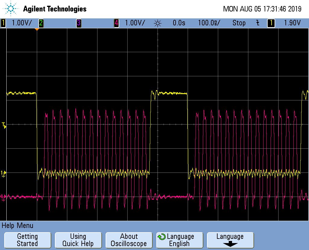
Here are some more details about how the parts are being used. The clock is 40 MHz with 50% duty. CS is low for 380ns and high for 120ns. The clock idles low, then it is pulsed 14 times after CS is asserted. CS rises after the falling edge of the 14th clock. I have checked the timing against the datasheet and don't see any violations. Also, the signals look clean without significant overshoot or ringing.

PDEN, CHSEL, AIN1N and AIN1P are not used and tied to ground. The part is used with AVdd=5V, DVdd=3.3V, Vref=4.096V

  • Hello,

    Do you have a pull up resistor on the CS lines?

    Thank you for the detail, but an oscilloscope shot of the digital communications would be best to diagnose possible sources.

    I suspect you will likely need to reset the device to get it out of this unknown state.

    Regards

    Cynthia

  • Hi Cynthia,

    The hardware does not have pull-up on CS or SCLK. They are open circuit for a second until the FPGA is configured, then CS is driven high and SCLK driven low.

    I am attaching an oscilloscope photo of CS and SCLK. These are the same waveforms whether the converters are emitting data or not. At the moment the converters are starting up normally so I can't show SDO, but it would be stuck at "0" permanently.

    I would be happy to reset the ADS7947 so long as it is something that can be done with CS and SCLK. Those are the only two inputs to the converter that I have available. I am not finding anything in the datasheet about reset. Is there a procedure ?

  • Hello ? Cynthia ?

    I would like to know more about the conditions that can lead to the chip getting stuck in a non-working state, and how to reset it.

    Thanks!

    George 

  • Hello George,

    Thanks for the scope shot, like you said this is correct behavior. A scope of what happens when the SDO line gets stuck would be what is needed, to see if the digital lines are still behaving correctly.

    I would recommend adding a pull up on CS, this way the device is powered up in a known state, and would eliminate the possibility of entering 32 bit mode. As long as the FPGA does not output anything on this line while power up.

    Would you clarify when exactly is this happening? You mention it is at start up, but it doesn't always happen. Are you power cycling the entire circuit, or just the FPGA while the ADC is still powered up?

    Also, can the FPGA you are using support all four data converters at full throughput? Could you start up the FPGA first and then bringing up the surrounding circuitry. 

    Regards

    Cynthia

  • Hi Cynthia,

    When the part is in the bad mode, SDO is stuck at ground and never moves off ground. We could add a straight line to the scope shot with a pencil and ruler and label it SDO. The digital lines are a pattern that the FPGA plays out which does not depend on SDO. This happens infrequently at startup and affects all four converters the same way. Once they get into this mode they never recover until a power cycle and restart. If they do start correctly, then they never fall into this state. I have not tried just reloading the FPGA. Also have not tried starting the FPGA first since they share the 3.3V power. Handling four converters at full speed is nothing for the FPGA - it has dedicated logic to do the job.

    A pull-up on CS would be an interesting experiment but the design is already in production. We would have to rework hundreds of boards, so to justify that we would need to be certain about cause and effect. Reprogramming the FPGA could be much easier.

    Along that line, here's an interesting thing that I learned about this problem. I wrote a new version of the FPGA that always generates 16 clocks instead of 14 clocks. In a week of casual testing with hundreds of power cycles, I have never seen this problem occur. The datasheet says that it is OK to stop clocking after the 14th clock, which is what the old FPGA did. I wonder if there is a corner case where that the 16 clocks avoid, or if the 16 clocks clear the part from 32b mode. It is not clear to me from reading the data sheet how to exit 32b mode, or I would also try that.

    George

  • That is an interesting find: I will look into the 14 clock pulse vs the 16 clock pulses with our designers. Do you see that once the device is started up using 16 SCLK, and then switch to use 14 SCLK pulses instead, the device behaves normally?

    The screen shot would be very helpful if you use it to capture it at start up when the SDO line gets stuck low. This will show at what state each digital line is at during starting up.

    The CS pull up would be helpful, but this can also be achieved by making sure the state of CS at start up from the FPGA is high.

    When the SDO is stuck low, have you confirmed that it in fact is in 32 bit mode by continuing to clock out pulses keeping CS low? Is data available on SDO after the 16SCLK?

     Regards

    Cynthia

  • Hi Cynthia,

    I have not tried switching between 14 and 16 clock pulse mode. My original logic only used 14 clock mode, then I rewrote it to only use 16 clock mode. Since this is all custom logic written in Verilog, it would be a little bit of a project to go back and try the test to see if it was in fact stuck in 32b mode by generating more clocks. Also, I could not get the necessary conversion rate in 32b mode so it would only be useful as at startup or as an experiment to better understand the problem. I lept to that conclusion since the behavior during the initial 14 clocks was SDO driven low, which is what the datasheet says that the part does when in 32b mode. I am engrossed in another aspect of the project at the moment but will go back to sample the state of the lines at startup. There is no more that I can do with the FPGA since it wakes up with all IO lines configured as inputs. Only after it is configured can I make the lines outputs, and then CS is driven high. The ADC will have been powered up for a second before the FPGA is configured.