This thread has been locked.

If you have a related question, please click the "Ask a related question" button in the top right corner. The newly created question will be automatically linked to this question.

ADS1230: ADS1230 didnt work correctly even with datasheet schematic

Part Number: ADS1230

HI 

I want to work with ads1230 with my processor(stm32f103)

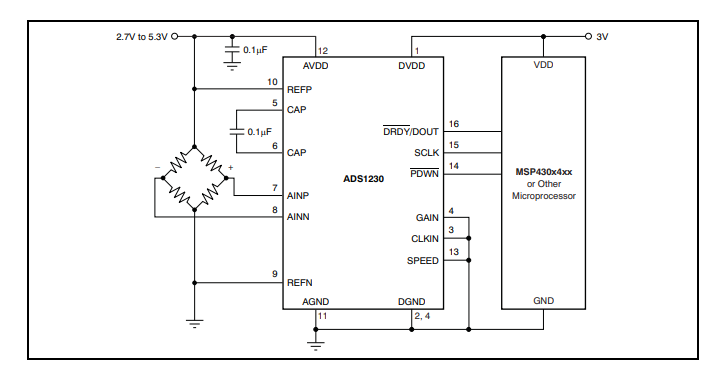
SCLK pin Clocks are fine , 20 clocks for data conversion and 4 additional clocks to force the Dout pin goes Hi

i saw the Dout pin and sclk pin on oscope , they are fine but Always ads1230 returns zero or constant number.

pdwn pin also connected in 2 ways :

1- the same as datasheet

2- connected to processor and handle it in software mode

VDD = 3.3V           VSS = GND

beside i measured the AINP and AINN pins they have 1.65V 

is there anything that i have to do!?

i apologize for my bad english

regard

  • Hi Iman,

    Welcome to the E2E forum!  I would suggest that you use the micro to control the PDWN pin and make sure that both AVDD and DVDD are at the nominal operating voltage for at least 10us before setting PDWN high.  All digital input pins must be connected and not left floating.

    Are AVDD and DVDD connected to the same 3.3V supply source?  Are AGND and DGND tied together?  Do you have a bridge sensor or load cell connected to the ADS1230 inputs?  Is the sensor excitation and ADS1230 reference all powered from the 3.3V source?  

    Can you send me scope or logic analyzer shots of the SPI communication?  Do you have pictures of your setup that you can share?

    Best regards,

    Bob B

  • Hi Bob

    AVDD and DVDD connected to same 3.3V,yes AGND and DGND tied together.I connected load cell to ADS1230. yes the sensor excitation and ADS1230 reference all powered from the 3.3V source. Dout and SCLK signal in scope and setup circuit  are attached. Do you have any suggestion schematic circuit for this issue?
    Best regards,
    Iman Sedaghat
  • Hi Iman,

    The scope shot is showing 0x80000 which is negative full-scale.  Usually this means a poor connection or missing reference voltage.  It is also possible that you have incorrectly wired the load cell to the ADS1230.  Measure the voltages at the device pins of the ADS1230 and make sure you are seeing the correct voltages at each pin.  If this a prototype board, such as a breadboard, it is very easy to make a mistake in wiring the connections, or have a wire come loose.

    Can you tell me some specifics about the load cell such as sensitivity (mV/V) and full-scale rating?  Can you tell me what wire colors of the load cell are connected to each pin/voltage?

    Best regards,

    Bob B

  • Hi Bob,

    thanks for your response


    I changed ADS1230 and resolder the pins also checked the wires and connections, now i get values that seems to be correct but i have 2 new problems!

    1- when i disconnected the oscop probes sometimes i got bad data! (for example every 10 correct data i got 1 bad data) then i checked the oscope outputs and i found this note (1MOhm || 13pF) so i put a 20pF capacitor near to SCLK pin of my MCU now that this issue disappeared! but why?!

    2-now i want to tare my Loadcell but i cant! i dont know why this happened!!

    our Load cell is Zemic L6D with output sensetivity 1.944mV/V and capacity of 50k

    Red Wire : Connected to refp also connceted to 3.3V
    Black Wire : Connected to refn also connected to Gnd
    Green Wire : Connected to AINP
    White Wire : Connected to AINN

    can we achieve a 1gr or under 1gr precision?!

  • Hi Iman,

    I’m glad to hear that you are making progress. However, it does appear that you are picking up noise in your wiring. It is going to be difficult to achieve high levels of performance without using a proper PCB layout with a solid ground plane. Any external wiring, such as load cell wiring, should be shielded wire and properly terminated at the PCB.

    To achieve 1g resolution you need to have 50,000 noise-free counts from the ADS1230. The noise performance of the ADS1230 is given in tables on page 6 of the ADS1230 datasheet. The lowest noise is achieved using the lowest data rate and the highest gain. This information is given in the table in the peak-to-peak noise column. For the calculation we will use Table 2, gain of 128 (GAIN pin high) and 10sps data output rate. The table shows 17.2 bits noise-free can be achieved.

    Scale resolution can be determined by using the formula shown on page 20 to determine noise-free counts. For a 1.944mV/V sensitivity and 3.3V excitation, the full-scale output of the load cell is 6.415mV and the full-scale range of the ADS1230 is +/-0.5*3.3V/128 which is 25.781mV. Using the formula for noise-free counts on page 20, this would equal 2^17.2(6.415mV/25.781mV) or 37,463 which would give us less than 1g resolution. With some averaging we may achieve another bit, which could possibly increase the resolution to 74,927 noise-free counts and would give 1g or better resolution.

    This is the best the ADS1230 can do, and excludes any noise from external sources such as EMI/RFI. The external noise sources are usually what cause the most issues. To help lower the external noise you could add some additional filtering to the analog inputs in the form of RC low-pass filters. You could start with the R values in the 1k to 4.7k range, and the C should be placed across the inputs and you can try values in the range of 10nF to 100nF.

    Best regards,

    Bob B