This thread has been locked.

If you have a related question, please click the "Ask a related question" button in the top right corner. The newly created question will be automatically linked to this question.

ADS8509: Noise on the ADC input when the converter starts working

Part Number: ADS8509
Other Parts Discussed in Thread: ADS8681, ADS8685, ADS8689

Hi TI technical experts,

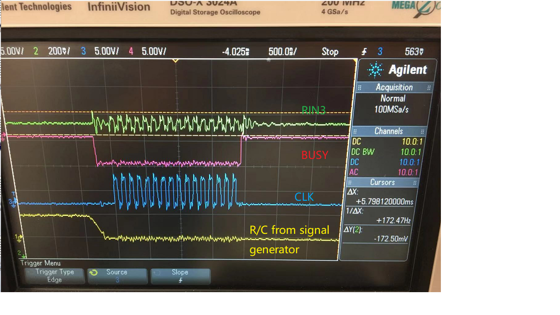
i met a problem when using ADS8905, it looks like crosstalk on the ADC input when the converter starting conversion or transfer data.

To debug this issue, I used a signal generator to triger the R/C through a opto-coupler, so the external GND is isolated with the ADC GND, please see attached schematic, and set the converter in internal clock mode, so i can detect the clock output, please see the picture. The ADC input started swing when R/C goes low, and was stable after the CLOCK output completed. This's weired, I don't know why, could you please advise? Thanks.

Jane

  • Hi Jane,

    ADS8509 is a switch-capacitor input structure SAR ADC. A falling edge on R/C signal puts the internal sample-and-hold circuit into the hold state and starts a conversion, so the BUSY will go to low to indicate this state and remain low until the conversion is completed. The internal switch will open or close for comparison and bit decision according to the internal clock, this is what your are seeing on the input, this is normal behavior for switch-capacitor input structure SAR ADC. Usually, a front-end driver with proper RC filter is required to drive this kind of ADC. TI Precision Labs - ADC training series has detailed introduction about this structure and design guide.

    Thanks & regards,

    Dale

  • Hi Jane,

    If your design is a new design, ADS8681 family is a good solution,  below are key features:

    • 16-Bit ADC With Integrated Analog Front-End (AFE)

    • High Speed:

    • ADS8681: 1 MSPS
    • ADS8685: 500 kSPS
    • ADS8689: 100 kSPS

    • Software Programmable Input Ranges:

    • Bipolar Ranges: ±12.288 V, ±10.24 V, ±6.144 V, ±5.12 V, and ±2.56 V
    • Ranges: 0 V–12.288 V, 0 V–10.24 V, 0 V–6.144 V, and 0 V–5.12 V

    • 5-V Analog Supply: 1.65-V to 5-V I/O Supply

    • Input Overvoltage Protection: Up to ±20 V • On-Chip, 4.096-V Reference With Low Drift

    • Excellent Performance: – DNL: ±0.4 LSB; INL: ±0.5 LSB – SNR: 92 dB; THD: –107 dB

    • ALARM → High, Low Threshold

    • multiSPI™ Interface With Daisy-Chain

    Regards,

    Dale

  • Hi Dale,

    Thank you very much for the reply, it helps a lot! I'm figuring out a proper RC filter for to reduce the noise. 

    And we do have a plan to refresh this old design in a year, yes, ADS8681 is a good solution. I will consider using it in the new design as you suggested. 

    Thanks&Regards,

    Jane