This thread has been locked.

If you have a related question, please click the "Ask a related question" button in the top right corner. The newly created question will be automatically linked to this question.

ADS1299: ADS1299 Signal noise ratio

Part Number: ADS1299

Hello:

   I am using ADS1299 to design the acquisition of eeg signals,I have some doubts and hope to get your company's support.

The hardware I designed is as follows:https://e2e.ti.com/support/data-converters/f/73/t/820794?tisearch=e2e-sitesearch&keymatch=ADS1299 

First of all, I used a sine wave of 400mV and 50hz to verify that it was correct.I then added a low-pass filter with a gain of 2 and a 50hz t-notch filter  (including REF electrode and BIAS electrode) to each channel.

But there is a problem. Does the BIAS electrode also need to add a low-pass filter with a gain of 2 and a 50HZ t-notch?

I have done a test. If the BIAS only adds low-pass filter with gain of 2, without t-trap, the signal is better, but I don't know whether there is theoretical basis for this?

The second problem is the low signal to noise ratio of the output signal,How can I change it to improve it?

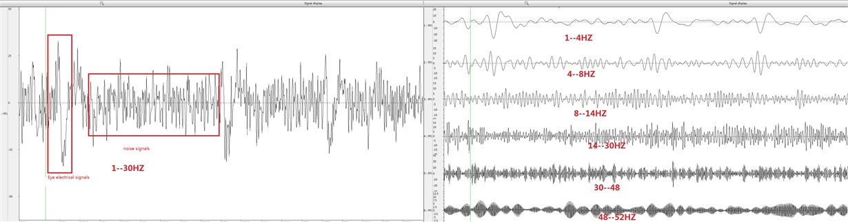
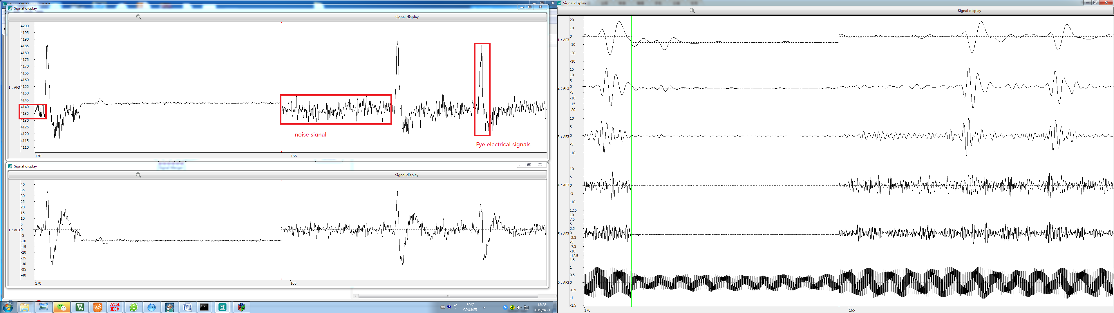
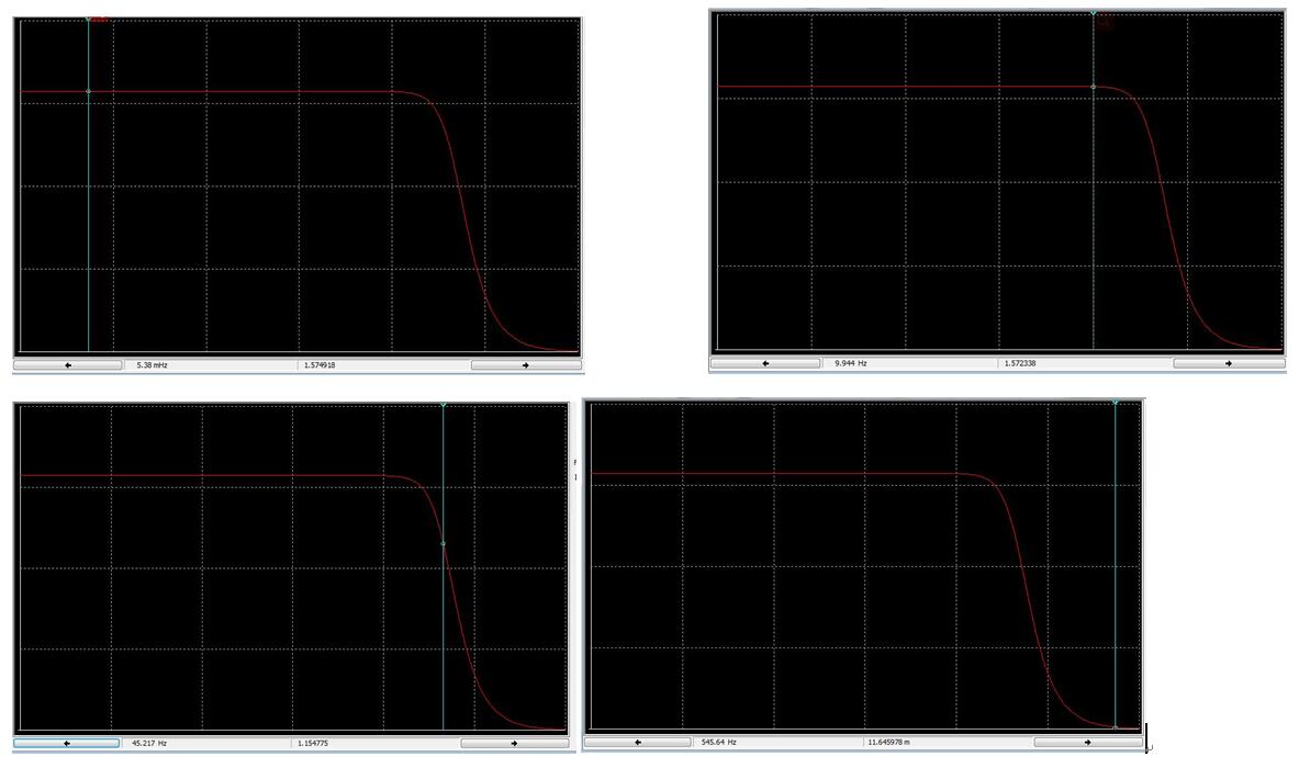
  • Waveform diagram is as follows:
  •  The standard waveforms of eeg products are as follows:
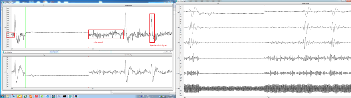
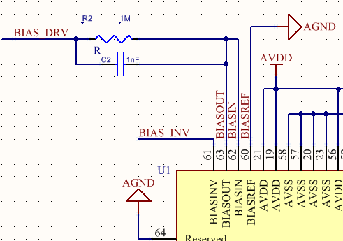
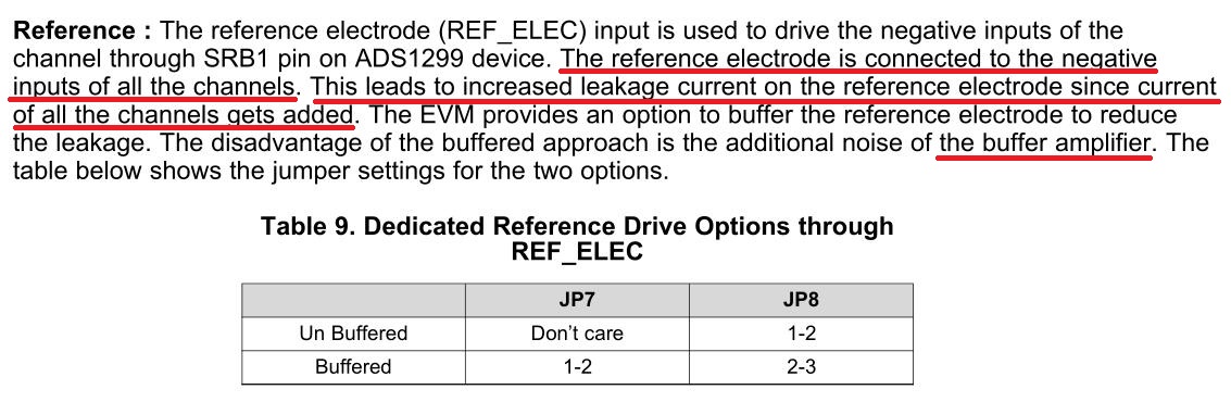
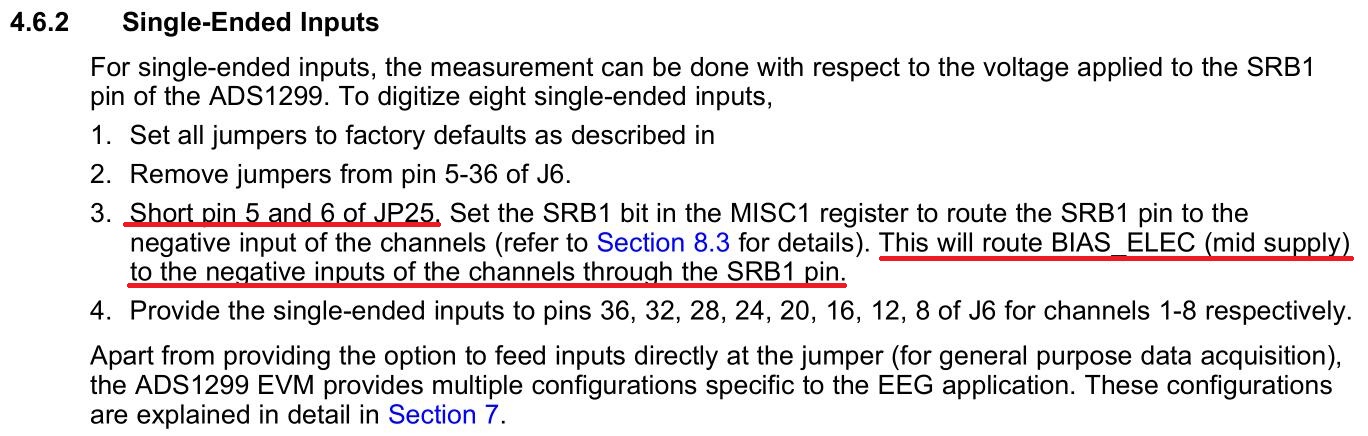
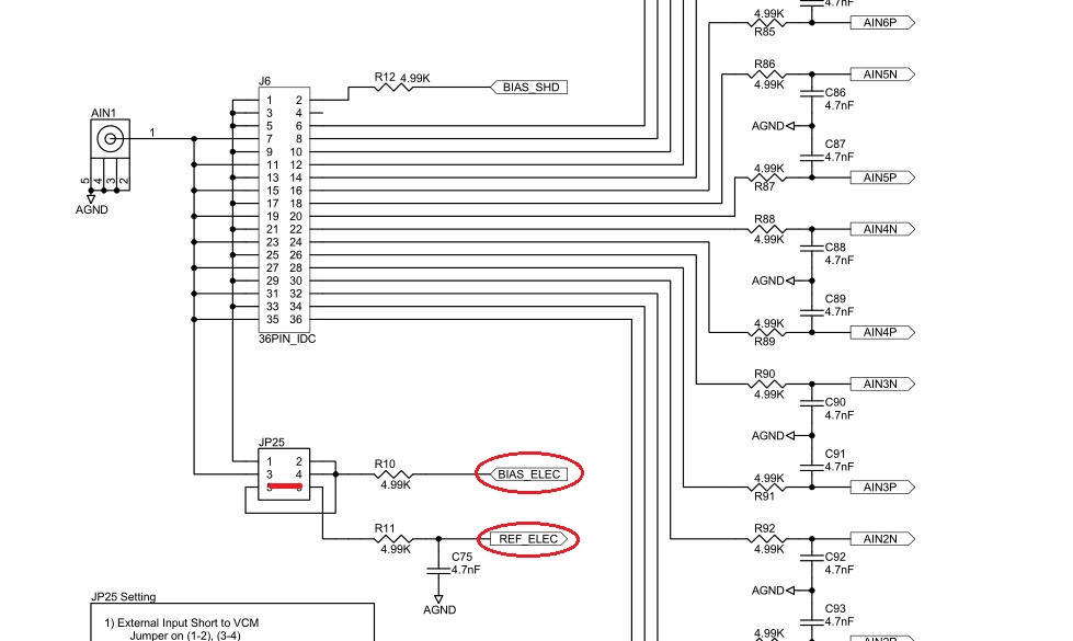
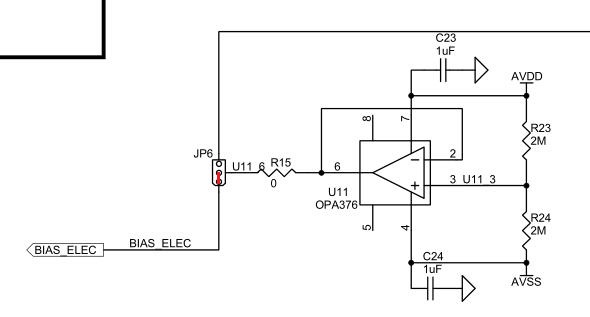
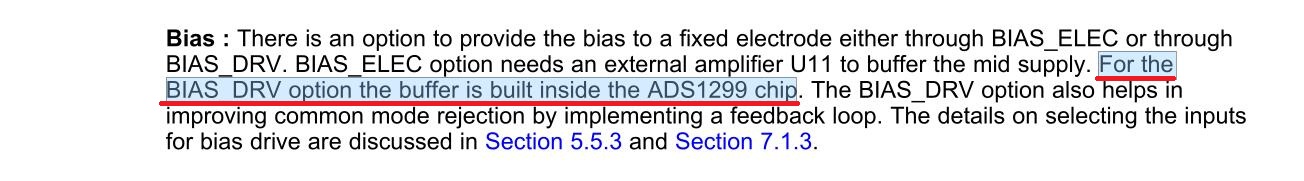
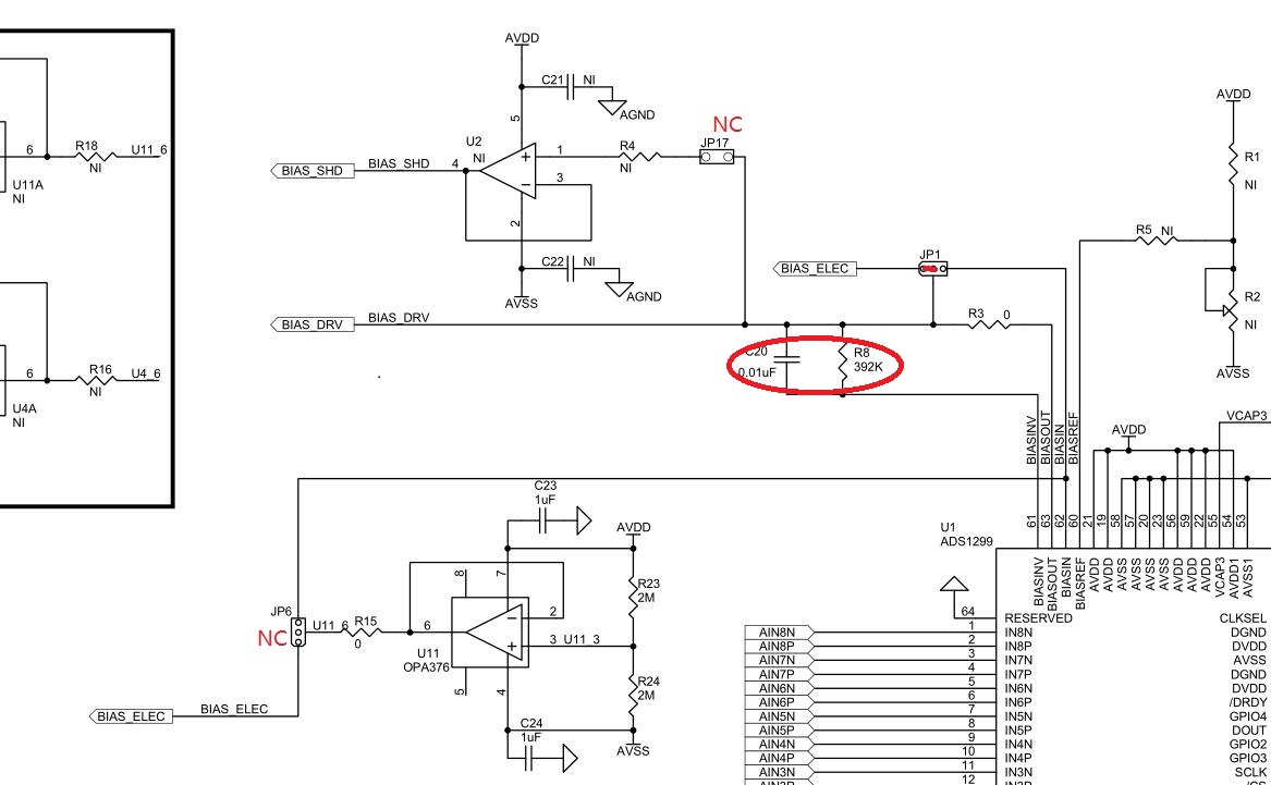
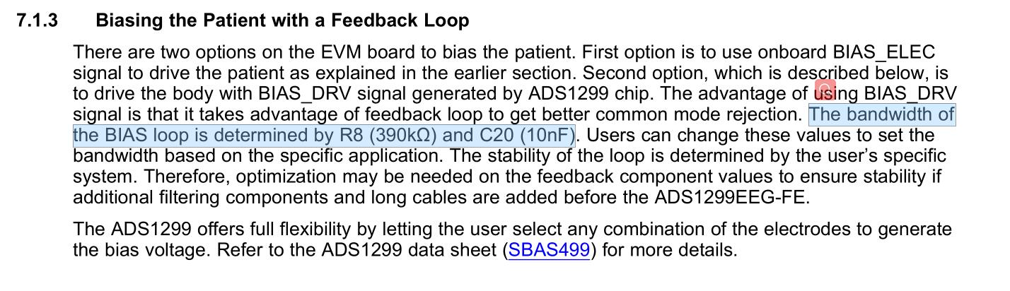
  • The third question is The hardware setup of BIas
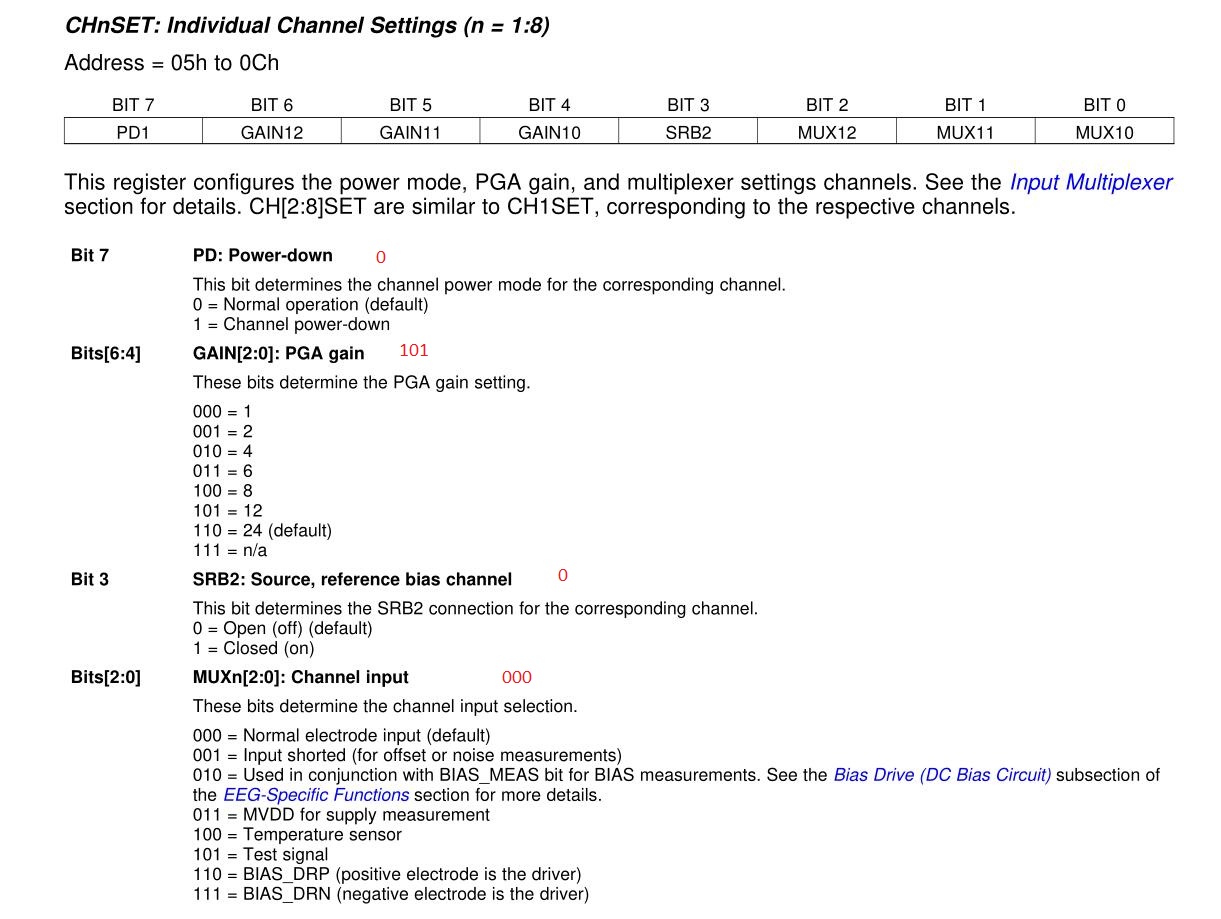
  • openbci setting as follow:
  • ADS1299 datasheet set as follow:
  •  

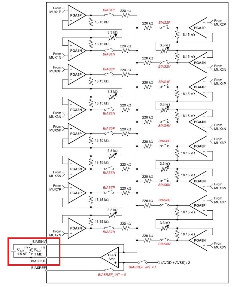
I would like to ask what is the advantage of this setup in openbci?Or is there any basis for that?  Which setting should I choose? Can you give me some advice?

thanks a lot !!


  • Hi,

    I apologize for not catching this in the last post, but it looks like your BIAS drive circuit is setup incorrectly. Please refer to the schematic at the end of this document: http://www.ti.com/lit/ug/slau443b/slau443b.pdf

  • Hello, thank you very much for your reply, I read the reference design document you recommended to me. I have some questions and really appreciate your help!

    Q1:about Reference electrode

       As shown in the red line above, The reference electrode (REF_ELEC) input is used to drive the negative inputs of the channel through SRB1 pin on ADS1299 device, This leads to increased leakage current. Do I have to add this buffer amplifier? If I don't add it, What are the implications?

    Q2: about bias :I think patient bias signal flow direction:  ADS11299--> patient , Is that right?

    bias signal purpose: The patient bias signal is used for biasing the patient to set the common mode of the EEG signals (typically mid supply).(P32 of  reference design) 

    Q3: about bias :Single-Ended Inputs setting about bias signal,BIAS_ELEC short to REF_ELEC, In this case, do I only need to connect to the patient's ear papillae via the 2 or 4 pin of JP25 (BIAS_ELEC)? What is this voltage value about mid supply?


    Q4: As for bias singnal, I adopted BIAS_DRV scheme, but I have some questions about it. I connected BIAS ELEC(2/4pin of JP25) to the ear papillae of the patient, I attached the REF ELEC(6pin of JP25) to the other ear papilla of the patient, Single-Ended Inputs setting. Is it right?

    Is there a formula for R8 and C20?

    What value should the bandwidth be set to?


    Q5: Can you check if my hardware configuration is correct?

      The hardware is modified as follows: as follows:

    Single-Ended Inputs:

       Set the SRB1 bit in the MISC1 register to route the SRB1 pin to the negative input of the channels.


    Risigter Setting: CONFIG1:0x01 0x96:1, 0, 0, 1, 0, 1, 1, 0

    CONFIG2:0x02 0xc0:1, 1, 0, 0, 0, 0, 0, 0

    CONFIG3:0x03 0xec:1, 1, 1, 0, 1, 1, 0, 0

    LOFF:0x04 0x00:0, 0, 0, 0, 0, 0, 0, 0

    CH1SET:0x05 0x50:0, 1, 0, 1, 0, 0, 0, 0

    CH2SET:0x06 0x50:0, 1, 0, 1, 0, 0, 0, 0

    CH3SET:0x07 0x50:0, 1, 0, 1, 0, 0, 0, 0

    CH4SET:0x08 0x50:0, 1, 0, 1, 0, 0, 0, 0

    CH5SET:0x09 0x50:0, 1, 0, 1, 0, 0, 0, 0

    CH6SET:0x0a 0x50:0, 1, 0, 1, 0, 0, 0, 0

    CH7SET:0x0b 0x50:0, 1, 0, 1, 0, 0, 0, 0

    CH8SET:0x0c 0x50:0, 1, 0, 1, 0, 0, 0, 0

    BIAS_SENSP:0x0d 0xff:1, 1, 1, 1, 1, 1, 1, 1

    BIAS_SENSN:0x0e 0xff:1, 1, 1, 1, 1, 1, 1, 1

    LOFF_SENSP:0x0f 0x00:0, 0, 0, 0, 0, 0, 0, 0

    LOFF_SENSN:0x10 0x00:0, 0, 0, 0, 0, 0, 0, 0

    LOFF_FLIP:0x11 0x00:0, 0, 0, 0, 0, 0, 0, 0

    LOFF_STATP:0x12 0x00:0, 0, 0, 0, 0, 0, 0, 0

    LOFF_STATN:0x13 0x00:0, 0, 0, 0, 0, 0, 0, 0

    GPIO:0x14 0x0f:0, 0, 0, 0, 1, 1, 1, 1

    MISC1:0x15 0x20:0, 0, 1, 0, 0, 0, 0, 0

    MISC2:0x16 0x00:0, 0, 0, 0, 0, 0, 0, 0

    CONFIG4:0x17 0x00:0, 0, 0, 0, 0, 0, 0, 0


    Thank you very much for your support!!!

  • Hi,

    1: It depends on how many electrodes you're measuring from and if you will be using lead-off detection or not. If you using all of the input channels and/or lead-off on multiple channels, then I would recommend adding the buffer. I'm not exactly sure where the "crossover" point would be as it depends on several parameters specific to your application. If the buffer is not added and you need it, then the voltage will droop and the noise will not be properly canceled. 

    2: Correct

    3: Correct, however keep in mind that the PDK is not intended for direct interface with a patient. 

    4: That is correct. For R8 and and C20, that's simply the feedback loop of the bias amplifier. A reasonable amount of gain at 60Hz is necessary to cancel the common-mode noise and specific values may need to be changed based on your specific application. 

    5: The inputs channels are currently powered down, I assume that's just when you took the register map and not for normal operation. 

  •    

    Hi Alexander Smith:

      Thank you very much for your reply!I still have some questions about your reply!

    1、Our current application is 8 channels acquisition, and in the future we will expand to 16 channels, 20 channels, 32 channels and even more channels, all with electrode shedding detection function!Is this buferr necessary for 8 channel acquisition devices with electrode shedding detection?

    3、Our equipment wants to be directly applied to patients. Can the hardware design scheme on Q5 be satisfied? What other peripherals do we add?

    4、For R8 and and C20, Is there a range of their values?

                        How can I verify that the value I modified meets the requirements?

    5、Can you check if my hardware configuration is correct about Q5?

       For Register setting , I checked it again, I think all eight channels are already powered on, Please help me to confirm it again, thank you!

       In fact, the most I want to know is whether my hardware design is wrong?

    Please help me to confirm it again, thank you!

  • Hi ,:

         Thank you very much for your reply!

    Based on the above Q5 hardware I added a preprocessing module, The specific design is as follows:

       Potential electrode-->Dual T-type 50Hz notch filte--> Second order active low pass filter (Fc=45Hz)--> ESD-->First-order passive low-pass filter -->INnP of ADS1299

       Ear papillae of the patient -->REF_ELEC--> Dual T-type 50Hz notch filte--> Second order active low pass filter(Fc=45Hz) --> -->ESD-->First-order passive low-pass filter -->SRB1 of ADS1299

       Ear papillae of the patient <--BIAS_ELEC <-- Second order active low pass filter(Fc=45Hz) <-- Dual T-type 50Hz notch filte<-- ESD<--First-order passive low-pass filter<--BIASOUT of ADS1299

    Q1:Is this hardware topology correct?

    Q2:Am I going to put a >100 operational amplifier behind the electrode?

    Q2: How to select operational amplifier? Can you specify it for me?

    Best regards!

  • Hi,

    1. You'll have to test as it depends on the specific electrodes and cables. 

    3. It looks fine, of course it can be pre-programmed as needed. I'm not sure what you mean by extra peripherals - it depends on your application and design. 

    4. I don't see R8 or C20 on your schematic, however I think you're talking about the RLD feedback loop in the user's guide. If so, it's important to have a significant amount of gain at 60Hz, and as mentioned in the user's guide the stability of the loop is determined on the specific system. Sticking with the user's guide values of 390kohm and 10nF should be fine for now. 

    5. You're right, I missed the first digit.

    The hardware looks fine. As long as you followed the user's guide there should not be an issue. When you have the layout, post it and I can take another look. 

    ~~

    1. I would not have such an aggressive cutoff frequency for the input filters. Inevitable tolerance mismatch in the filter components (namely the capacitors) will lead to different cutoff frequencies, and therefor different levels of attenuation based on frequency. This will create issues when the input signals differential is measured as the noise will not cancel out equally.  

    2. We do not recommend using an additional external amplifier. The ADS1299 has an internal gain of 24 which should be sufficient for measurements. The input signal may not use the full-scale range, however it will be a very low noise measurement - which means high SNR (signal to noise ratio). If an external opamp is used, the input referred noise of the opamp will be multiplied by the gain of the opamp, and then the gain of the ADC. Using the opamp will allow you to take advantage of the full-scale range, however most of the time the extra noise causes the SNR to decrease compared to the measurement without the opamp. If you must find an opamp, it should be very low noise. 

  •    

    Hi Alexander Smith:

      Thank you very much for your reply!I still have some questions about your reply!

    1、If you don't add this REF_buffer, what aspect of the signal does it affect?

       In the signal waveform, which part?

    3、By peripherals, I mean Sep 2, 2019 3:23 AM preconditioning module

    4、For R8 and and C20, R8 corresponds to R2 and C20 corresponds to C2 in the figure above,

    I want to have a significant amount of gain at 50hz.

       Q4_1:  How to choose the values of R8 and C20? Can you recommend them to me?

       Q4_2:  I'm talking about the right leg drive feedback loop, What I don't understand is the   relationship between the RLD and the measuring electrode and the reference electrode?

       Q4_3:  " The patient bias signal is used for biasing the patient to set the common mode of            the EEG signals (typically mid supply).(P32 of  reference design) "

            Is it "Common Voltage" in the red circle below?

          Reflected in the actual signal waveform, is this baseline in the red box below?Is that what we mean by radical drift?


     ~~

    1、I see what you mean,but I still have a little question.

       When referring to "cutoff frequency for the input filters", does it mean a notch filter, a low-pass filter or the whole preprocessing module?

    low-pass filter Amplitude-frequency characteristic diagram:


    Phase frequency characteristic diagram:

    As shown above, regarding the simulation graph of this low-pass filter, does the phase difference affect the signal quality greatly?

         Are you suggesting that I not add notch filters and second order active low pass filters to the analog end?Is it ok to add only a passive filter built with resistors and capacitors (reference in design)?In this way, the original output of ADS1299 will be a large amount of 50Hz power noise. If I want to filter it out, is it better to filter it out at the digital end and not at the analog end (electrode)?


    Best regards!!

  • Hi,

    1. It affects the integrity of the reference signal. If there is not enough drive strength the signal may begin to droop (lose magnitude). 

    3. I still don't know what this is. Pre-conditioning of what for what purpose?

    4.1 There are several documents on TI.com related to opamps. For now, I recommend just using what's on the EVM as shown in the user's guide or you can play with the TINA file from this thread: https://e2e.ti.com/support/data-converters/f/73/t/832614

    4.2  Video 1.4 of this series may help: https://training.ti.com/how-measure-ecg-introduction-what-ecg?cu=1128637 "BIAS" is known as "RLD" in ECG applications. The BIAS drive is pushing a common-mode voltage as well as the inverted noise signal onto the patient in order to keep the input signals within the common-mode range of the PGA as you are showing in your diagram, and to cancel out the 50Hz noise. The reference electrode is the "baseline" measurement. The measurement electrode is the "difference" measurement. At the input of the device, the difference positive "measurement electrode" and negative "reference electrode" is found. This essentially gives you the signal that is present between the two electrodes. 

    4.3 Yes, it could be a drift issue, offset, etc. 

    _______

    1. Low pass RC filter as shown in the user's guide. The phase doesn't matter as both input channels will see the same shift. It's best to let the BIAS drive handle the 50Hz noise. There is an app note in the BIOFAQ located in my signature that goes into this in depth, however for "RLD" not "BIAS". The principles of operation are the same. 

  •    

    Hi Alexander Smith:

      Thank you very much for your reply!I still have some questions about your reply!

    Q1: Do I need to add notch and active low pass filter (not RC filter) between the input of ADS1299 and the measuring electrode to reduce external interference to the device?

        If I add a 50hz notch to the measuring electrode and the input of ADS1299, do I add it to the reference electrical extremes?

    Add it on the BIAS_OUT side?

    Q2:Based on the above hardware Settings, I plan to add the function of electrode shedding detection.According to the reference design, there are two ways: dc lead-off and ac lead-off

    I measured these two modes: DC mode:


         ID:0x00 0x3e:0, 0, 1, 1, 1, 1, 1, 0

    CONFIG1:0x01 0x96:1, 0, 0, 1, 0, 1, 1, 0

    CONFIG2:0x02 0xc0:1, 1, 0, 0, 0, 0, 0, 0

    CONFIG3:0x03 0xec:1, 1, 1, 0, 1, 1, 0, 0

    LOFF:0x04 0x04:0, 0, 0, 0, 0, 1, 0, 0

    CH1SET:0x05 0x50:0, 1, 0, 1, 0, 0, 0, 0

    CH2SET:0x06 0x50:0, 1, 0, 1, 0, 0, 0, 0

    CH3SET:0x07 0x50:0, 1, 0, 1, 0, 0, 0, 0

    CH4SET:0x08 0x50:0, 1, 0, 1, 0, 0, 0, 0

    CH5SET:0x09 0x50:0, 1, 0, 1, 0, 0, 0, 0

    CH6SET:0x0a 0x50:0, 1, 0, 1, 0, 0, 0, 0

    CH7SET:0x0b 0x50:0, 1, 0, 1, 0, 0, 0, 0

    CH8SET:0x0c 0x50:0, 1, 0, 1, 0, 0, 0, 0

    BIAS_SENSP:0x0d 0xff:1, 1, 1, 1, 1, 1, 1, 1

    BIAS_SENSN:0x0e 0xff:1, 1, 1, 1, 1, 1, 1, 1

    LOFF_SENSP:0x0f 0xff:1, 1, 1, 1, 1, 1, 1, 1

    LOFF_SENSN:0x10 0x00:0, 0, 0, 0, 0, 0, 0, 0

    LOFF_FLIP:0x11 0x00:0, 0, 0, 0, 0, 0, 0, 0

    LOFF_STATP:0x12 0xff:1, 1, 1, 1, 1, 1, 1, 1

    LOFF_STATN:0x13 0x00:0, 0, 0, 0, 0, 0, 0, 0

    GPIO:0x14 0x0f:0, 0, 0, 0, 1, 1, 1, 1

    MISC1:0x15 0x20:0, 0, 1, 0, 0, 0, 0, 0

    MISC2:0x16 0x00:0, 0, 0, 0, 0, 0, 0, 0

    CONFIG4:0x17 0x02:0, 0, 0, 0, 0, 0, 1, 0


    The 8 electrodes tested are available, but the sensitivity is relatively high. It is considered to be effective when lightly applied to the skin. How to improve it?

    How does REF_ELEC test?(add buffer function to REF_ELEC in hardware design)

    How does BIAS_ELEC test?(according to the method given in the reference design, it doesn't seem to be suitable for the hardware I designed.)

    AC - leadoff:

    Methods: a resistance with an accuracy of 0.1% was bonded between the measuring electrode and REF_ELEC. The measurement was still accurate when the ac_lead-off mode was set. However, if I bonded the resistance with an accuracy of 0.1% between all 8 channels and REF_ELEC, the measurement result would be completely incorrect.

    How about BIAS_ELEC and REF_ELEC?

  • Hi,

    1. No, just an RC filter is fine. Other filters may have mismatches which lead to common-mode rejection issues.

    2. I don't understand what you mean by "high sensitivity" do you mean that it shows the lead is off when it's actually on but perhaps moved slightly? Using wet electrodes and/or using sandpaper on the skin can help improve the connection. 

    Are you saying that you connected all 8 channels together to one end of the resistor, and the REF_ELEC to the other end of the resistor? Make sure that the lead-off currents are balanced - they are not all negative or positive, but equal of each positive and negative magnitudes. Otherwise the BIAS_ELEC will have to source/sink the extra current to balance the measurement. 

    You may be interested in this article as well: https://www.planetanalog.com/signal-chain-basics-149-how-to-accurately-measure-electrode-impedance-for-lead-off-detection-in-ecg-systems/

  • Hello, thank you very much for your reply, I still have one more question. I hope you can help me confirm it.

    1、The working environment of eeg acquisition device (ADS1299) is servo motor equipment. The power frequency interference of 50hz is very large, with a peak-to-peak value of about 2mv. We want to reduce this interference in the hardware part (analog end), how to deal with it?

    2、We want to test the electrode impedance in real time, to indicate whether the patient's skin is in good contact with the electrode. In the case of AC square, how do I test the electrode impedance with precision resistance to simulate the electrode impedance?

    3、Single input mode,How is impedance measured with reference electrodes?There seems to be no reference in the manual.

    4、How is impedance measured with Bias electrode?