This thread has been locked.

If you have a related question, please click the "Ask a related question" button in the top right corner. The newly created question will be automatically linked to this question.

ADS8664: ADS8664 spi communication

Part Number: ADS8664

I use ADS8664 and want to communicate by spi.

I want to confirm the spi communication by read the default register value.

I wonder how i can read the default register value.

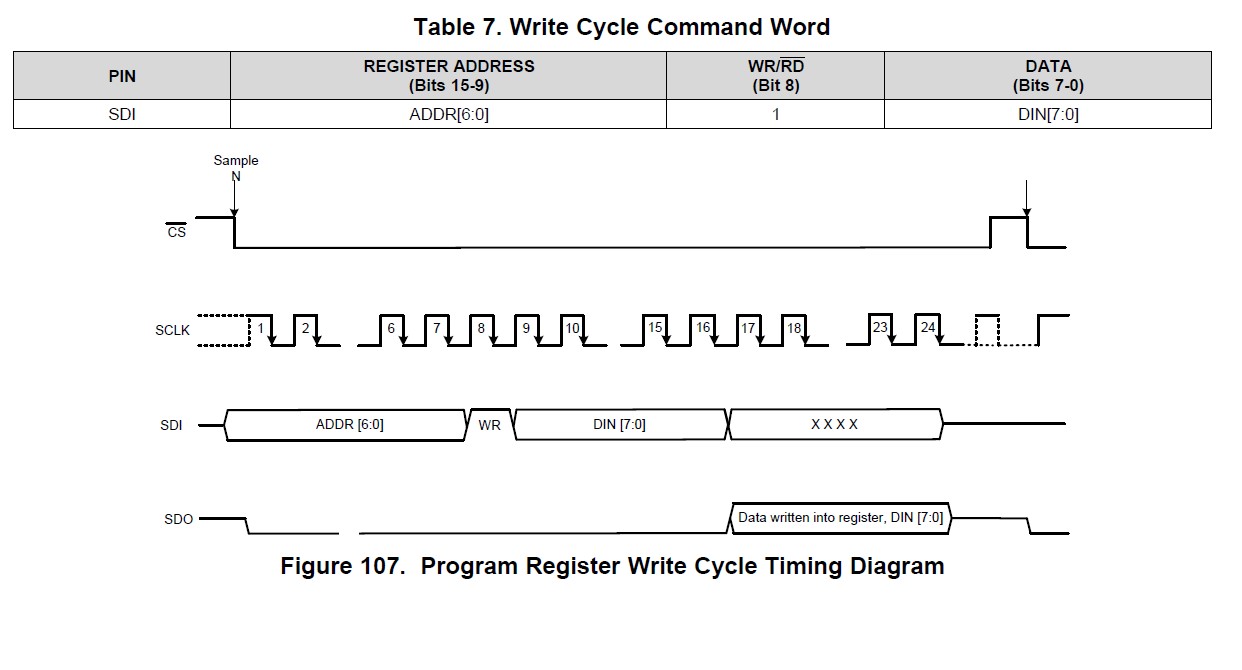
I try to spi in this way. the data send with MSB, and 32 bit(In the data sheet, The command or program register is 16 bit + additional bit 8. I just send more 8 clk.)

1. I send the command data as stanby_state = > 0x82000000

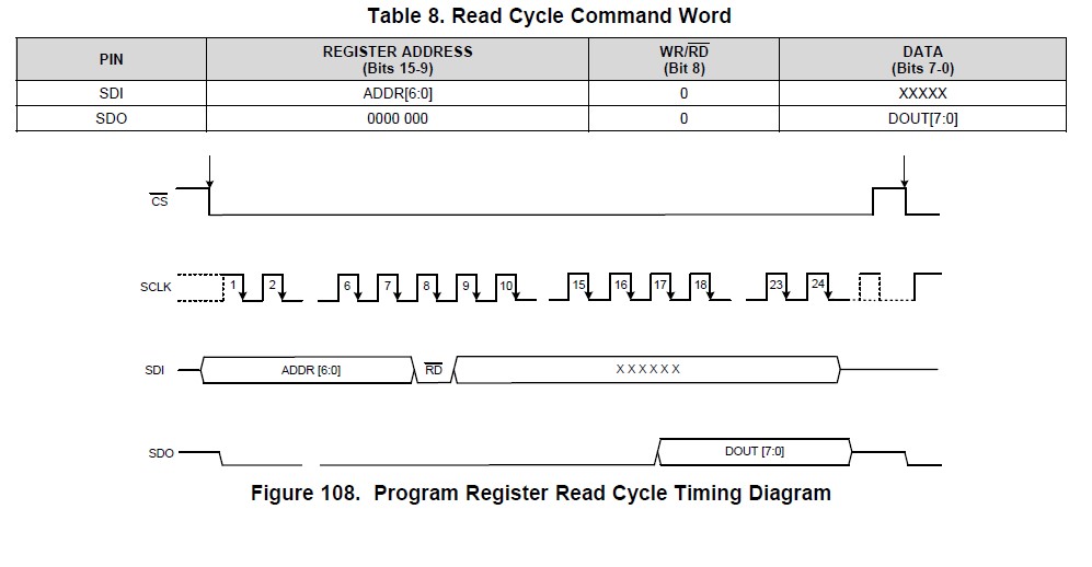
2. I send the program register read => 0x2E000000

   - the address 0x17 is located in 15:9 bit. So, left shift 1 bit is applied then the data is 0x2E.

3. Repeat process 2. with checking by wavefrom.  

I confirm the CLK, SDI and  CS are act well. but SDO is act strange. I want to know the way to contorl this chip.

  • Hello,

    This device has two types of registers 1. command registers and 2. program registers.

    1. The command register is for device sampling mode, standby, power down and rest

    2. The program register is for channel sequence, data format, analog input range, alarms features.

    When communicating with the device, I would suggest using an oscilloscope connected to the digital lines to make sure that the data lines are correctly doing what is expected. This will also help debug any issues and confirm SDI and SDO data.

    To read the program default program registers, a total of 24 SCLK pulses are needed after CS goes low. The below except from the datasheet will help to describe how to read a register


    Since you are trying to read the alarm threshold for channel one the first bits will be the address: 17h (0001 0111 b), but the register only takes 7bits, which means that the leading bit needs to be truncated. As you noted left shift would be needed, but this needs to be done in binary to make sure the shift is done correctly.

    This is then followed by a 0 to set to Read. After this, the bits are all do not cares, thus set to zero.

    This command, put together is then: 2E or (0010111 0 0000 0000b)

    ~This post has been updated for clarification. apologies for the confusion~

     Regards

    Cynthia


  • Hello, Cynthia

    I tried spi test follow your guide. But the spi miso is not act.

    The test method follows,

    1. I send data command 0x850000.

    2. Repeat send data 0x170000 (as guide)

    3. the result is miso data 0.

    The waveform like this - 0x170000 data.

    (yellow : MOSI, blue : CS, pink : CLK(about 110 ns), green : MISO)

    I have some question.

    1. If I want to read in 17h -> then I send 0x170000, Then, if I want to write in 17h, I send 97h. Is it right?

    2. If i want to use command, I send 24 clk or 16 clk or it is no matter?. and I send the data follow the table? (0x8500, 0xC000 ... etc)

    3. If i want to use program register. I just send the program register address in 16 bit? (0x01, 0x17 etc..)

    Regards,

    Minwoo

  • Hello,

    I made a mistake in my previous response, I have corrected it in the post.

    Now, that you have timing correct, I would suggest changing a program register. Then, try reading that same register to confirm that is has been changed to what you wanted to.

    To write to the program register, Bit 8 needs to be set to high. Thus (0010111 1 xxxx xxxxb) which is 2Fxxh.

    If you are writing to the program register, and not concerned about the conversion result that could be available in that frame, than 24 SCLK cycles are fine. If you still want the conversion results available at that frame, then 32 SCLK pulses are needed.


    To write to the command register, than a full 32 SCLK data frame is needed, and should follow Figure 1 in the datasheet.  This is a write only register.

    Regards

    Cynthia

  • Hi Minwoo,

    To read or write a program register, a minimum 24 SCLKs after /CS is required. Your command in your 1st post (0x2E000000) is correct to read the register High Threshold LSB register, the problem is, you put the device into standby mode by sending standby command (0x82000000). The 8-bit register data is expected to see at 17th-24th bit on SDO. 

    Regards,

    Dale