This thread has been locked.

If you have a related question, please click the "Ask a related question" button in the top right corner. The newly created question will be automatically linked to this question.

ADS5562: CLKout in SLOW SPEED MODE

Part Number: ADS5562

Hello,

I have a question about ADS5562.

<Customer Use Case>
- Sampling frequency: 12.5MHz
- LOW SPEED mode (Tying the SCLK pin to high)
- CMOS mode

[Q1]
Their CLKOUT (5pin) duty cycle is not 50%.
Their measurement result is about 78%.
Why is this?
Are there any possible causes for the above?

- D/S, p15, 6.11 Timing Characteristics for LVDS and CMOS Modes
  PARALLEL CMOS MODE: CMOS output clock duty cycle= 50%

<My thoughts>
The measurement conditions for the following data are Default Speed ​​Mode.
I think that it may not apply when used in Low Speed ​​Mode.

The important thing about CLKout is not the duty cycle but the rising edge.
Therefore, I don't think I need to worry about the Duty Cycle not being 50%.

[Q2]
I asked them to investigate the waveforms to see if they met the following conditions:
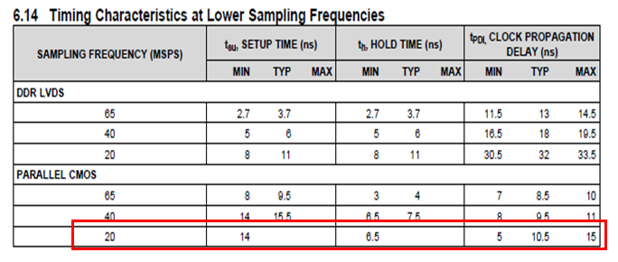
- D/S, p16, 6.14 Timing Characteristics at Lower Sampling Frequencies
- D/S, p18, Figure 5. CMOS Mode Timing

As a result,
tPDI = about 70ns.
tsu = about 25ns
th = about 55ns
This result does not seem to meet the requirements.

Why is this?
Are there any possible causes for the above?

Also, I think that even if the Output Clock Position is adjusted using the SEN Control Pin, the request cannot be satisfied.
What should I do?

Best Regards, 
Kaede Kudo

  • Kaede,

    Make sure the following conditions are meet:

    1. Reset pin is connected to 3.3V.  

    2. SDATA pin is connected to GND.

    3. SEN pin is connected to 3.3V

    4. DFS pins is set to either 1.23V (3/8 * DRVDD) or 2.06V (5/8 * DRVDD) for proper CMOS output mode.

    Regards,

    Jim

  • Jim, 

    Thank you for your reply.

    1. Reset pin is connected to 3.3V.  
    ->Yes. Reset pin is connected to DRVDD.

    2. SDATA pin is connected to GND.
    ->Open. But I think this is OK because it has an internal 100-kΩ pulldown resistor to DRGND.

    3. SEN pin is connected to 3.3V
    ->Open. But I think this is OK because it has an internal 100-kΩ pullup resistor to DRVDD.

    4. DFS pins is set to either 1.23V (3/8 * DRVDD) or 2.06V (5/8 * DRVDD) for proper CMOS output mode.
    ->DFS pin is set to 1.99V (5/8 * DRVDD).

    *DRVDD pin = 3.21V
    *AVDD pin = 3.2V

    They also checked the voltage on the OE pin.
    OE pin is set to open.
    OE pin = 2.36V

    As with the OE pin, the SEN pin that was pulled up to DRVDD internally and left open was also checked.
    SEN pin = 3.16V

    Best Regards,

    Kaede Kudo

  • Jim, 

    I'm sorry, but I am going to revise some of the previous answers.

    4. DFS pins is set to either 1.23V (3/8 * DRVDD) or 2.06V (5/8 * DRVDD) for proper CMOS output mode.
    ->DFS pin is set to 1.19V (3/8 * AVDD).

    Since they refer to the user guide circuit, they are connected to AVDD instead of DRVDD.
    But user guide circuit is ADS61x9.
    I think that DFS pin are connected to DRVDD.
    Is this a problem?

    Best Regards, 

    Kaede Kudo

  • Kaede,

    I do not think this is a problem. I would suggest changing the DFS to (5/8 * AVDD) and verify the output switches from 2's complement to offset binary.

    Regards,

    Jim

  • Kaede,

    Can you make changes to SEN per the data sheet to see if the CLKOUT moves with respect to the input clock?

    Another thing that may be an issue is that the reset input must wait a minimum of 5ms to go high after power is applied (Figure 1 of the data sheet). Do you have a way to delay the reset as it appears to be connected to 3.3V directly? 

    Regards,

    Jim

  • Jim, 

    Thank you for your reply.

    I gave them your comments.
    No feedback from them.

    However, I think the reset timing is the cause.
    As you comment, they are pulling up the Reset terminal to power.
    I think that the problem can be solved by improving the timing of Reset.

    Thank you for your cooporation!

    Best Regards, 

    Kaede Kudo