This thread has been locked.

If you have a related question, please click the "Ask a related question" button in the top right corner. The newly created question will be automatically linked to this question.

ADS8556: ADS8556 power-down mode

Part Number: ADS8556
Other Parts Discussed in Thread: ADS8555

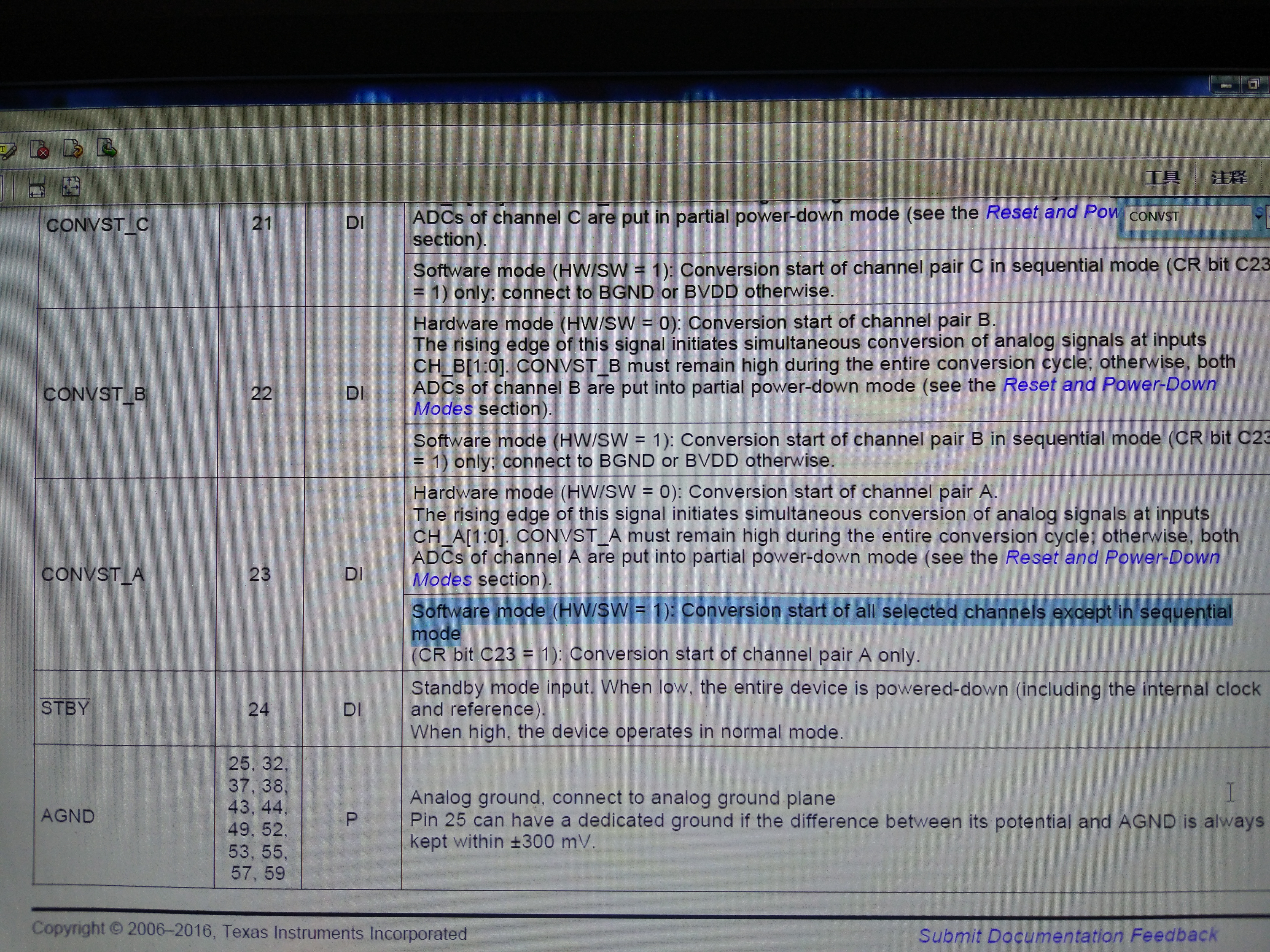
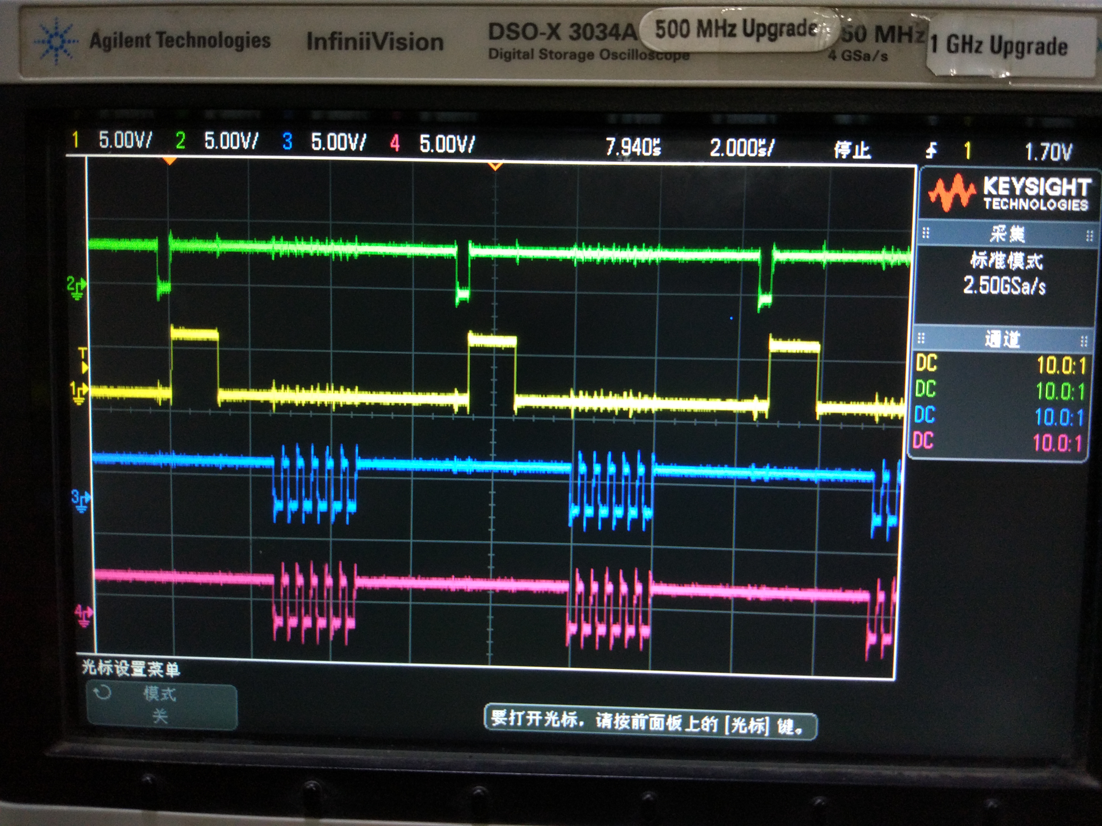
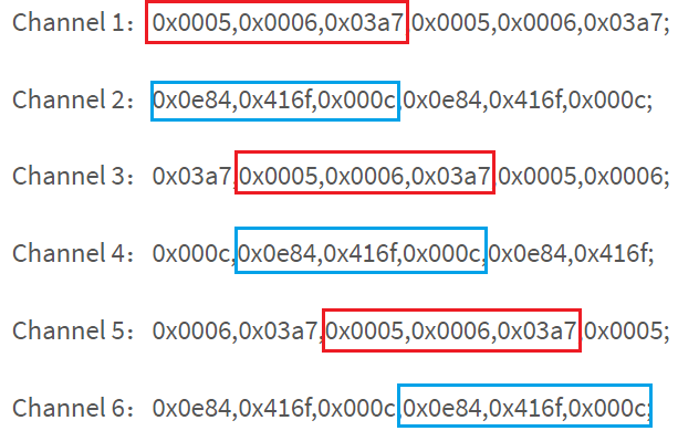
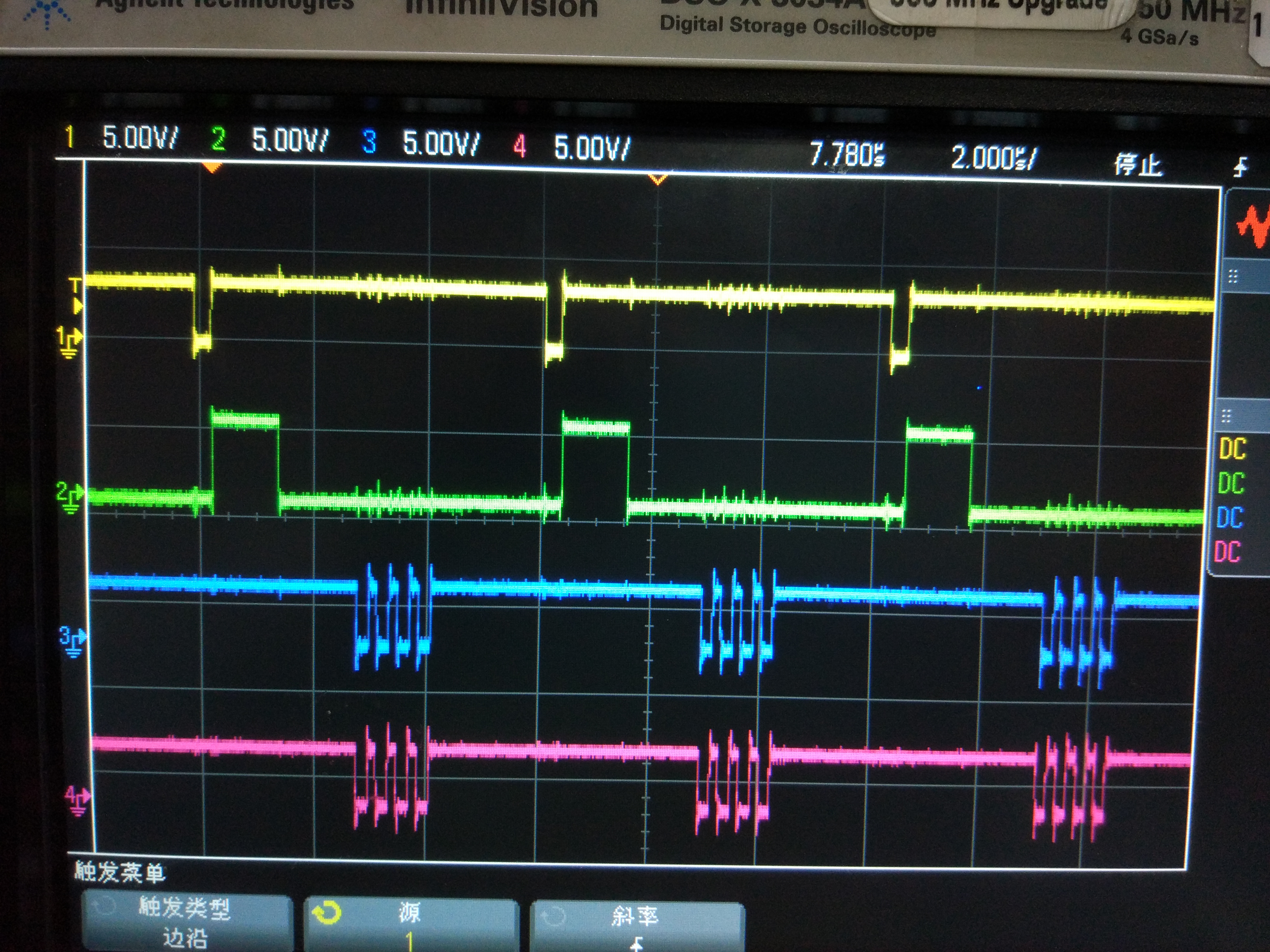
hi,from the datasheet,bring the convst signal low during an ongoing conversion when busy signal is high can put ads8556 into power-down mode. Is there any other reason can put ads8556 into power-down mode beside this?

  • Hello user3783133,

    I have responded your previous query. We can keep communication in one thread. Your timing plot will be very helpful to address the issue.

    Based on your description,it is very likely that your device has entered partial power-down mode. ADS8556 ADC will detect CONVST_x signal at the falling edge of BUSY signal, the device will enter this mode if CONVST is low or the device will continue next conversion if CONVST is high at this moment. Usually, CONVST_x signal is recommended to pull down after low BUSY signal is detected by microcontroller, a low BUSY also means that the conversion has been done.

    Do you need power-down mode for power-saving? 

    Thanks&regards,

    Dale

  • Hello Dale,

    Thank you very much for your reply.I have measured the time sequence, which is correct and consistent with the requirements of the datasheet. I don't need power-mode.  This just happens occasionally in the normal operation of the system, and the probability is very small. And I want to know what causes this situation except for the reasons you mentioned.

    Thanks&regards.

  • Hi user3783133,

    Based on your description, the device should be in partial power-down mode either by pulling down CONVST signal on the falling edge of BUSY (this reason was eliminated if your timing was correct as you said) or interference signal to CONVST. I suggest you can try two experiments:

    • Add a pull-up resistor on CONVST_x signals to DVDD, you can ignore this suggestion if you have done it.
    • Use ADS8555 which is pin-pin also software compatible to ADS8556, however the  partial power-down is not available on ADS8555.

    Thanks&regards,

    Dale

  • Hello Dale,

    Please consult again. When the device has entered power-down mode, and then I send CONVST signal again. At this time, the data I read is as follows:

    Channel 1:0x0005,0x0006,0x03a7,0x0005,0x0006,0x03a7;

    Channel 2:0x0e84,0x416f,0x000c,0x0e84,0x416f,0x000c;

    Channel 3:0x03a7,0x0005,0x0006,0x03a7,0x0005,0x0006;

    Channel 4:0x000c,0x0e84,0x416f,0x000c,0x0e84,0x416f;

    Channel 5:0x0006,0x03a7,0x0005,0x0006,0x03a7,0x0005;

    Channel 6:0x0e84,0x416f,0x000c,0x0e84,0x416f,0x000c;

    As you can see,the value of each channel is three cycle values and there is also a certain relationship between channels.

    Is this normal? What's the reason for this?

    Thanks&regards.

  • Hi user3783133,

    More information will be helpful to understand the issue. Did you send 6 CONVST_x signals to ADC when the issue happened? Did you connect all three CONVST pins together or not? What's your input on each channel when you got these data results? Was your reference voltage on REFIO pin correct when you got these results? How about the BUSY signal after you sent these 6 CONVST_x signals to ADC? Did you observe any interference signal on CONVST_x or /RD signal?

    Thanks.

    Best regards,

    Dale

  • Hi Dale,

    1.  Yes,I send  6 CONVST_x signals to ADC when the issue happened.And if I continue to send  another 6 CONVST_x signals to ADC,I can get the same result as above;

    2. I use software and 16bit-parallel mode to access ADS8556,CONVST A is connected to the controller and CONVST B/C is pulled down.

    The schematic diagram is shown in the attachment.

    3. For channel 1 to channel 4 , The input is the sensors’  output signal,the inputs of channel 5 channel 6 are +5V power supply and AGND;

    4.The reference voltage on REFIO pin (2.5V) is always correct.

    5.After I sent these 6 CONVST_x signals to ADC,there is no BUSY signal output every time;

    6. I didn't observe any interference signal on CONVST_x or /RD signal;

    When the issue happened,if I reset  and then reinitialize(write 0xe00003fff to Configuration Register) ADS8556,the collected data can be restored to normal.

    Thanks&regards.

  • Hi Dale,

    There's another information to explain.

    As you can see,the power supply of BVDD(Pin 9) is +5V,but my controller is powered by 3.3V,can this cause ADS8556 to enter power-down mode?

  • Hi user3783133,

    Your CONVST_B and CONVST_C pins are connected to ground, so the ADC should not have conversions on channel pair B and C, how could you get the data for channel pair B and C? How many /RD pulses with one /CS low after you sent one CONVST_A signal to the ADC? I really need your timing plot (/CS, CONVST,BUSY and /RD) for one and two frames to check.

    Is there any capacitor on REFIO, REFCAPA0,REFCAPB0 and REFCAPC0 pins?

    It's good to apply different constant DC voltages you have known to inputs so that you can check the conversion codes easily.

    Your 3.3V digital logic will not be able to bring the ADC into power-down mode, you may worry about the microcontroller because 5V logic level from ADC may damage the digital input on your microcontroller.

    Thanks and regards,

    Dale

  • Hi Dale,

    From ADC datasheet,CONVST_A can start all six channels in software mode,so I only used CONVST_A.

    When the system is working normally,my timing plot is as follows:

    Channel 1 is BUSYsignal,Channel 2 is CONVST_A  signal,Channel 3 is /CS signal,and Channel 4 is /RD signal.

    For REFIO, REFCAPA0,REFCAPB0 and REFCAPC0 pins,all these pins are decouple with a 10uF and a 0.1uF capacitor.

    Please help me to confirm whether there is any risk in the timing plot.

    Thanks and regards.

  • Hi user3783133,

    Thanks for your timing plot and information.

    1. For CONVST_A signal, you are right, thanks.
    2. Your are reading the data during acquisition time, your timing is good at normal condition and did not violate the timing required.

    If we check the data you captured, we can find that actually only 6 data were shown on these 6 channels periodically, see the highlight in red and blue color below: 0x0005,0x0006,0x03a7, 0x0e84,0x416f,0x000c. Notice that the data shifted to bus depends on the /RD pulses you send to the ADS8556 ADC. To read the data correctly for total 6 channels, 6 /RD pulses during one conversion/acquisition frame should be exact and restricted, otherwise the data order will be messed up.

    Hence, I think firstly the ADC has entered either Partial Power-Down mode or latch-up which can stop the conversion and stop outputting BUSY signal. An interference signal to CONVST_A at the moment of  falling edge of BUSY can lead to Partial Power-Down mode, the interference signal can be very short and not easy to be observed. After the ADC enters the Partial Power-Down mode, the ADC will stop working and will always output the last conversion data to the data bus. This is the reason why we only see 6 constant data on the bus of ADC. I suggest you:

    1. Get ADS8555 sample for the test which is exactly same as ADS8556 only except Partial Power-Down mode.
    2. Use pull-up resistor connecting to DVDD on the CONVST_A signal, this resistor should be close to the ADC.

    Secondly, please check your software and make sure it does not output more or less than 6 /RD pulses in every frame. I suggest to a pull-up resistor on /RD and /CS signals which should be close to the ADC. Also, it is good to have a small resistor (49.9ohm or 33ohm) in series with /RD,/CS and CONVST_A signal.

    Please let me know your test result and further question if you have.

    -----------------------------------------------------------------------------------------------------------------------------------------------------

    ----------------------------------------------------------------------------------------------------------------------------------------------------

    Thanks&regards,

    Dale

  • Hi Dale,

    Based on your description, if the ADC has entered latch-up it can also stop the conversion and stop outputting BUSY signal.I want to know what causes the ADC to  enter latch-up mode.

    Thanks&regards.

  • Hi Dale,

    Based on your description, if the ADC has entered latch-up it can also stop the conversion and stop outputting BUSY signal.I want to know what causes ADC to  enter latch-up mode.

    Thanks&regards.

  • Hi user3783133,

    Latchup can be caused by a number of triggering factors including overvoltage spikes or transients, exceeding maximum ratings, and incorrect power sequencing. It can happen at any place where the required parasitic structure exists including on an input or output. Latch-ups can be caused by a trigger including current injection or overvoltage. However, I think the first step is to verify if this was caused by Partial Power-Down so ADS8555 was strongly suggested for you. 

    Regards,

    Dale 

  • Hi Dale,

    As you said,my 3.3V digital logic will not be able to bring the ADC into power-down mode.But from the datasheet,the minimum value of High-level input voltage is 0.7xBVDD(3.5V),so this is certainly a theoretical risk but in practice there is no problem.

    So,what's the real minimum value of High-level input voltage or the true scale factor between minimum value of High-level input voltage and BVDD?

    Thanks and regards.

  • Hi,

    There are only three digital input signals to the ADC with parallel interface on this ADC: /CS,/RD and Convst_x, the ADC worked well based on your timing and information showed. If you have any concern about this, why do not you use +3.3V for BVDD on pin 9 instead of +5V? it will be simple and the +3.3V power for digital power supply of this ADC will perfectly match the +3.3V signals from your microcontroller.

    I'm looking forward to hearing back from your experiments regarding my suggestions.

    Regards,

    Dale

  • Hi Dale,


    Thanks for your reply.I have confirmed that 3.3V digital logic will not be able to bring the ADC into power-down mode.

    There are two more questions I will consult you again.

    1.I only use four channels  in practical engineering application,so after each data conversion,I send  only 4 /RD signals to ADC.In theory,is there any risk in this way of reading?
    Timing plot is as follows:

    In the picture above, the signals from top to bottom are /CONVST,BUSY,/CS,/RD.

    2.If I bring the CONVST signal low during an ongoing conversion when BUSY signal is high and bring the CONVST signal high before the falling

    edge of BUSY signal(timing plot is as follows),in theory, is there any risk in this case?

  • Hi user3783133,

    1. I did not see any risk to use 4 channels on this ADC.

    2. I did not see any risk regarding your description about CONVST, actually I did the same test 10 year ago and no issue was found. However, this is not suggested because your system should be a robust system to cover all conditions including over temperature, any variation on your timing may lead to a worse result including power-down. Hence, monitoring BUSY to read the data and bring CONVST to low is always recommended.

    Regards,

    Dale