This thread has been locked.

If you have a related question, please click the "Ask a related question" button in the top right corner. The newly created question will be automatically linked to this question.

ADC12J2700EVM: connected to a Xilinx Kintex Ulstrascale + KCU116 dev board

Part Number: ADC12J2700EVM
Other Parts Discussed in Thread: LMK04828

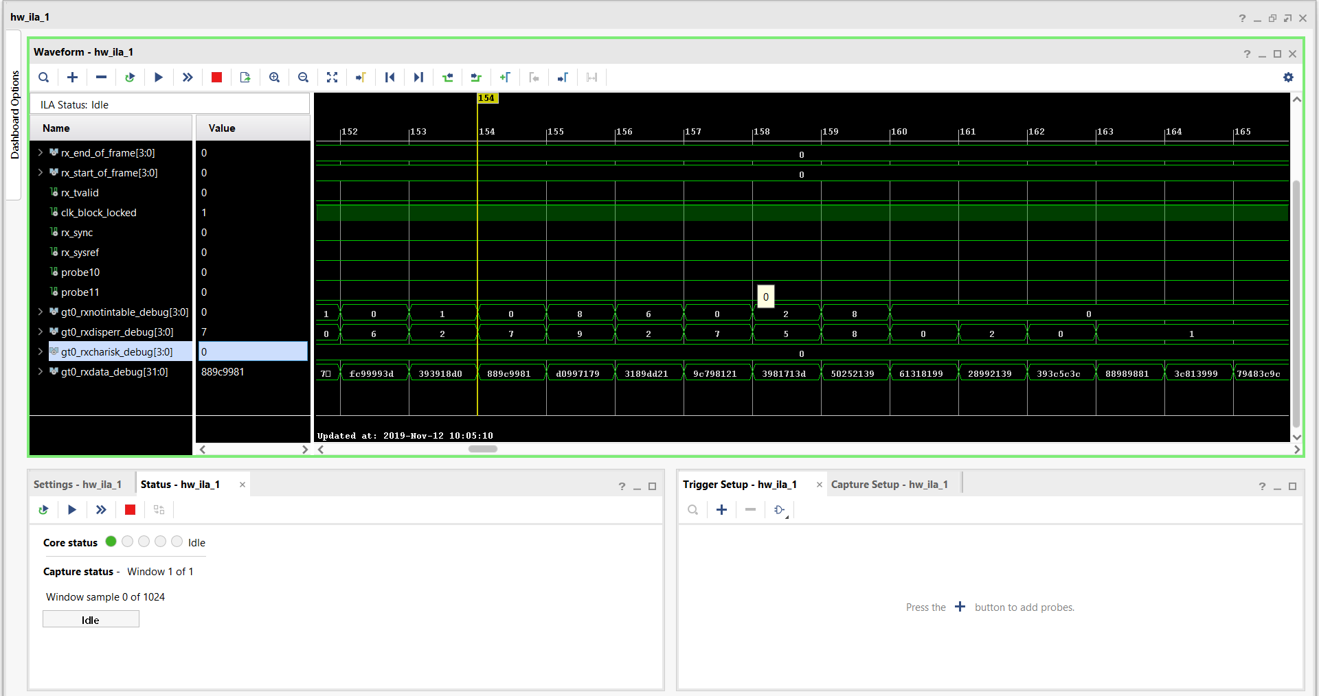
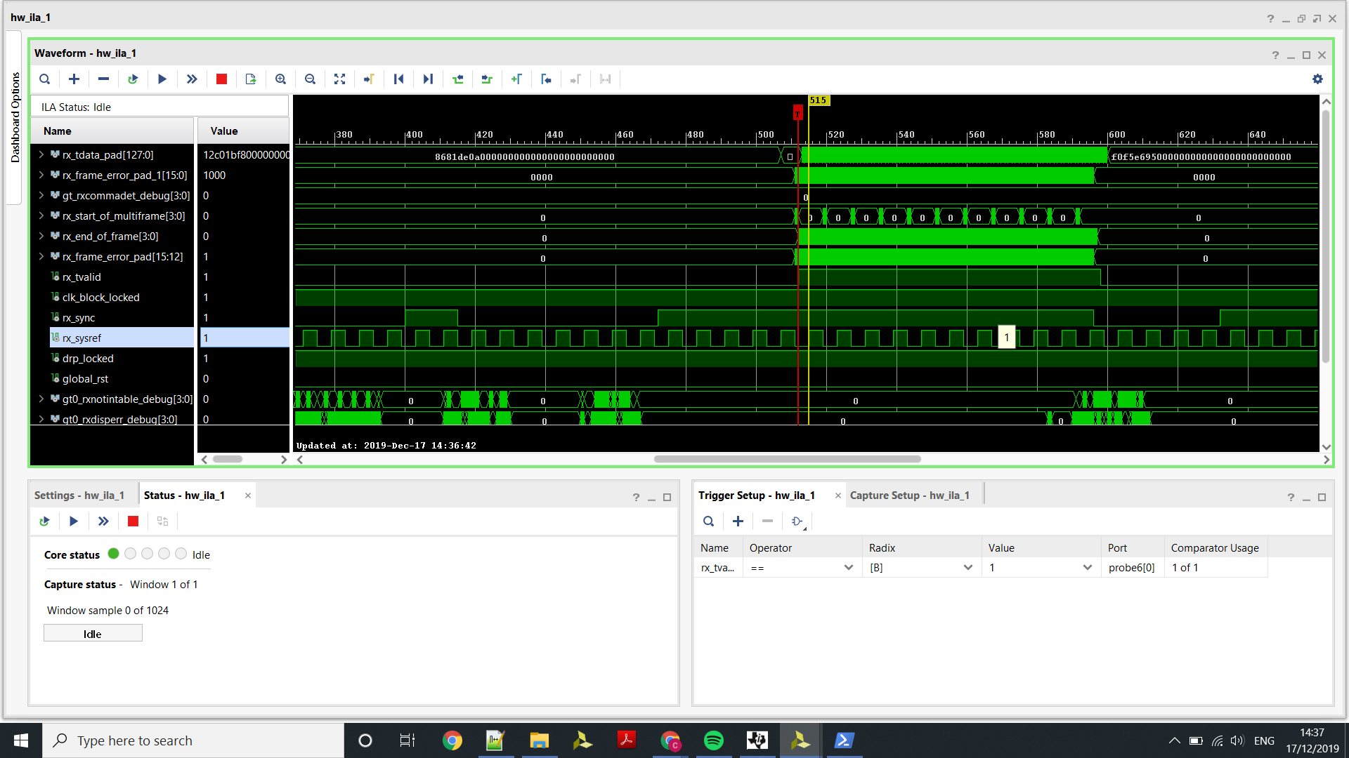
i want to connect the ADC12J2700EVM to a Xilinx Kintex Ulstrascale + KCU116 dev board , i want to run the ADC in 12 bit bypass mode, however the dev board only has 4 transceiver pins through the FMC connector will i still be able get data through the JESD204b receiver in the FPGA with only half the lanes active? 

  • Charles,

    For bypass mode, you will need all 8 lanes. See Table 11 of the data sheet.

    Regards,

    Jim

  • Hi Jim,

    Are you saying it wont work at all or i will only receive half the data?

    it doesn't really matter at this stage at least what the data is, i just need to get something, i am simply trying to demonstrate that i can get data.

    Regards,

    Charles

  • Charles,

    You can get data from the converter using 4 lanes, but you will lose half of the samples. Looking at Table 13, you can see what samples you would get depending on which lanes you are using. Foe example, if you are using lane 0, you would get sample 0, sample 8, sample 16, sample 24 and sample 32.

    Regards,

    Jim 

  • Hi Jim

    what is the reference frequency for the FPGA transeiver if i use on board clocks and set the ADC to 1.6 GSPS?

    Regards

    Charles

  • Charles,

    I am guessing it will be 80MHz but I am not 100% sure as we have not tested this setup with this platform at this data rate. When using the ADC12J2700EVM with a KCU105 wit the ADC sample rate at 3100MHz, the FPGA reference clock was 3100 / 20 = 155MHz.

    Regards,

    Jim

  • Hi Jim,

    So i'm struggling a bit with this, could you check my figures for me?

    i have the JESD204B receiver set up to resync the lmfc each time it receives the SYSREF

    the DEV CLK/Sample clock is running at 1.6 GHz

    the FPGA ref clocks are 200 Mhz (divide by 8) and 100Mhz (divide by 16)

    I'm using 4 lanes i have the ADC set to Decimation = 4 , DDR =1 PS5 =1 (2.5x) as this mode used only 4 lanes (so transceiver bit rate is 4Gbs)

    L = 4

    M = 2

    F = 2

    K = 32

    S = 2

    JESD Frame clock = Sample Cock / S = 800 Mhz (this seems wrong but that's what the datasheet says)

    LMFC = 25Mhz

    SYSREF Period = K*F*4*DEVCLK Period = 32*2*4*0.625 = 160 ns

    SYSREF freq = 6.25Mhz (1/160 ns)

    this means on the LMK0482 chip the divider needs to be set to 256 , i have it running in continuous mode

    Determistic calculations (taken from xilinx document pg066-jesd204)

    Tlmfc = 40 ns

    Twire = 0 (assumed)

    ADC characteristics

    Ttxlmfc = 25 ns

    Ttxout = 32.9375 ns

    Ttxin = 40ns

    JESD204B on Xilinx

    Trxlmfc = 40ns

    Trxin = 150-170ns

    Trxout = 0

    N = 4 was chosen

    max latency = 32.9375 + 0 + 170 < (((4+1)*40) -25 + 40)

    min latency  = 32.9375 + 0 + 150 > ((4*40) -25 + 40)

    Tlatency = 5*40 - 25 + 40 + 40 = 255 ns

  • Charles,

    What is the issue? Is the link not getting established? If so, what is the status of SYNC? Is it toggling? Is the FPGA reference clock 200MHz or 100MHz? Is the FPGA really using a core clock? Have you consulted with Xilinx about this?

    Regards,

    Jim

  • Hi Jim

    well i'm not sure exactly what the issue is  
    the LMK0482 supplies both ref clocks over the FMC connector, the first one is the DEVCLKARX on the schematic which is the transceiver ref clock and runs at 200Mhz
    the second is the  DEVCLKBRX which i have running at 100Mhz and is synchronous with the SYSREF that the chip also sends out over the FMC connector.
    I don't know if ~SYNC being set i only have one going to the ADC itself connected and not the LMK0482 chip (this pin is not connected on the xilinx board)
    the clocks are operating correctly in the FPGA as i'm driving some user logic with them and chip scope.
    I haven't contacted xilinx 
    Regards
    Charles
  • Charles,

    What firmware are you using? The JESD204B SYNC that is connected between the ADC and FPGA can be monitored by using the Xilinx Chipscope tool. Have you tried this? You can also monitor the data lines to verify the K28.5 characters are coming across from the ADC during CGS.

    What version is the ADC EVM and what version of the GUI are you using? There is a chance you may be running with the wrong GUI version.

    Regards,

    Jim

  • Hi Jim

    so i was using the wrong version of the gui , which wasn't helping

    i may need to talk to xilinx about this but im' hoping you can help as well

    so i've made some progress on this im getting data out of the phy but im getting disparity errors , which i'm not exactly sure what that means.

    i have a 1.6Ghz sample clock  i have k = 32 and f= 2 and m = 2 ,i think my LMFC period is 25 mhz , but again not sure due to how terrible all the documentation on the standard is! i set the sysref signal to 6.25mhz from the clock controller (so every 4 multi-frames i get sysref), i don't get any sysref capture errors.

    if send test k28.5 pattern on the adc side i clearly get a repeating pattern in the fpga but its not the repeating pattern i expect and then after a few clock cycles it will change to another repeating pattern.

    the sync will assert but then stay asserted and the adc then just continues to send a repeating pattern in normal mode. do you have any ideas what i'm doing wrong?

    i think i'm not aligning stuff correctly but its soo difficult to debug the interface.

  • Charles,

    If the FPGA asserts SYNC low, then receiving the K28.5 characters on all lanes, after it receives a minimum of 4 K28.5 on all lanes, the FPGA should send SYNC high. If it is not sending this high, the problem is usually an issue with the reference clock, SYSREF or the firmware. With your clock rates mentioned above, the LMFC should be 12.5MHz. If SYSREF is at 6.25MHz, then this is correct. Can you verify if the reference clock is the correct frequency the firmware needs?

    FYI, the serdes data lines P/M out of the ADC are swapped so you will need to un-swap them in the FPGA.

    Regards,

    Jim  

  • Hi Jim

    the reference clock for the transceiver is 200Mhz (sample clock divided by 8), 

    then i have another clock coming from the lmk04828 chip which is 100Mhz (sample clock divided by 16) and is source synchronous to the SYSREF  also coming from that chip, if i set it to 6.25mhz the fpga registers tell me its able to capture it correctly

    but i'm still seeing disparity errors and the SYNC coming out of the fpga is just always lo

    i'm not  running in bypass mode though , i'm running with decimation of 4 this is because it uses only 4 lanes so the ddr =1 and ps5 = 1 which means each lane is running at 4Gbps

    i tried swapping p/n  on the transceiver pins but that didn't work in fact it looked worse so i think they were correct to begin with

    Regards 

    Charles

  • Charles,

    For a sanity check to verify the ADC is programmed properly, after you load the registers and provide a clock, input a 500MHz tone at 0dBm to the VIN SMA. If the ADC is operating properly, both over range LED's should be on. When you lower this amplitude to around -3dBm, one of the LED's should turn off. If you lower the input to -5dBm or less, both LED's should turn off.

    The Altera firmware we use on our capture board only requires a reference clock, and with your settings, this is 100MHz. Is there a chance your firmware needs this to be at 100MHz instead of 200MHz?

    Regards,

    Jim 

  • Hi Jim,

    So i'm understanding the protocol a lot better now and the more in understand it the less i understand why my stuff doesn't work!

    the data coming out of the PHY is wrong , and get a bunch of disparity errors. This is before any of the protocol stuff.

    i expect to see the K28.5 character of "BC" repeatably but i don't, instead i get garbage. the sync is low so its still in the CGS stage of initialisation.

    now what is interesting is if i invert the p and n pins in my FPGA device and tell the ADC jesd204b to send the K28.5 test pattern. i start getting a more repeatable pattern say "47" or "82" but its still not "BC" this i find to be very strange. sometimes i do see "BC" in the data but not reliably.

    if i hook up p/n the ways its stated in the user guide and turn the jesd204b interface on and off in adc gui , the transceiver just continues to give me garbage almost as if its not connected.

    however with pins inverted to what is stated, if i toggle the ADC's jesd204b on then i get a repeatable pattern and if i turn it off i get zeros which is more sensible.

    these are the pins i have assigned in my fpga

    set_property PACKAGE_PIN A3 [get_ports {x_rxp[3]}]
    set_property PACKAGE_PIN B1 [get_ports {x_rxp[2]}]
    set_property PACKAGE_PIN C3 [get_ports {x_rxp[1]}]
    set_property PACKAGE_PIN D1 [get_ports {x_rxp[0]}]
    set_property PACKAGE_PIN A4 [get_ports {x_rxn[3]}]
    set_property PACKAGE_PIN B2 [get_ports {x_rxn[2]}]
    set_property PACKAGE_PIN C4 [get_ports {x_rxn[1]}]
    set_property PACKAGE_PIN D2 [get_ports {x_rxn[0]}]

    this is what i believe to be correct when compared to the schematic but if i invert these it seems to look more sensible (although still not working).

    any ideas?

    here is the chip scope

    the SYSREF was turned off during this capture 

    Regards,

    Charles

  • Charles,

    Try the following: Program the ADC to operate at the lowest sample rate. Next take a speed scope probe, and probe the serdes lanes using the capacitors on the bottom of the board near the ADC. With SYNC low, the K28.5 characters (0xBCBC) should be constantly coming out all of the lanes. This is pretty easy to observe with a scope probe when the serdes rate is low. See the attached document for what this should look like in 8b/10b mode. I have also attached a debug document as well that may help.

    Regards,

    Jim

      K28.pptxJESD204B Bring UP and Debug.pptx

  • Hi Jim

    so i measured the data lines coming out of the adc the capacitors on the diff lines , and the frequency seems to be a factor of 20 out , so if i put it 1000MSPS i get 100Mhz when i expect 2GHz (DDR =1) if i set it to 1600MSps i get 160Mhz when i expect 3.2 GHz , what am i missing?

    edit : it might be the probe i was using wasn't able to deal with those line rates

    Regards,

    Charles

  • Charles,

    I was on vacation so I was unable to reply earlier. Can you verify the ADC clock is at the expected frequency? Can your scope measure a signal that is 2GHz? I cannot think of anything else that may be an issue. Did the ADC pass the LED test I described in an earlier post?

    Regards,

    Jim 

  • Charles,

    I would suggest you get Chipscope up and running inside of Vivado so you can monitor the activity on each lane along with SYNC and SYSREF.

    This will allow you to verify if all four lanes are transmitting the K28.5 (0xBCBC) characters while the SYNC is held low by the FPGA.

    Regards,

    Jim   

  • Hi Jim,

    so i got the JESD204b working! or at least i now see data on the FPGA user side which i think means its synced up and gone through all the stages, i ran the ADC at 1 GSPS and 1 lane and it seemed to spring into life so there it clearly too much noise/ cross-talk or something for these 2 boards to work together at higher speeds and more lanes!

    Also the lanes are not reversed n=>p p=>n like the specification says, so i'm not sure whats going on there.

    Regards,

    Charles

  • Correction they are reversed

  • Charles,

    If using decimate by 4, you will need to program the NCO to get a valid output. The NCO frequency will be subtracted from the input tone. So if you are sampling at 1Gsps, the ADC output data rate will be 250MHz. The 1st Nyquist zone will be 125MHz. If you input a 200 MHz tone, then set the NCO to 100MHz to get a 100MHz output. Give this a try.

    Note that the device will pass CGS (SYNC going back high) if the lanes are swapped as this does not change the K28.5 pattern. We have done this in the past.

    Regards,

    Jim

  • Charles,

    As a sanity check, after you program the ADC, give it an IF at 500MHz @  2dBm. You should see two over range LED's turn on. Slowly lower the amplitude of this input until both turn off. I think this will be around -5dBm. This is a good test to verify the ADC board is working properly.

    Make sure you are programming the ADC in decimate-by-4-DDR P54 mode when using the ADC GUI. Once you start sending a tone to the ADC , you will then need to set the NCO so that the tone falls in band of the ADC (0-200MHz).  

    Regards,

    Jim

  • Charles,

    I would suggest having the FPGA hold SYNC low and monitor the ADC output lanes. Leave SYNC low until all four lanes are sending valid K28.5 characters.

    Once you have passed this step, have the FPGA send SYNC high. Using Chipscope, trigger on a rising edge of SYNC.  After the next LMFC rising edge after SYNC goes high, the ILA data sequence shall start. Monitor the four lanes during the ILA sequence. You should start seeing data that looks familiar to the data in the attachment.

    Regards,

    Jim

    7870.ILA example LMFS_8244.pptx  

  • Hi Jim,

    i have attached some screen shots to show where i am with my progress essentially i can now get the SYNC to toggle high but it toggles for a few clock cycles before falling out of sync , some times it gets further and the jesd204b even outputs data. what do you think? this is with the adc running in bypass mode F=8 k=4 scrambler =on

  • Charles,

    Now that you are using bypass mode, can you answer the following:

    ADC sample rate

    SYSREF rate

    FPGA reference clock rate

    HD parameter (this should be 1)

    Can you disable any settings that would reset the SYNC if the ILA sequence fails inside the FPGA?

    Regards,

    Jim 

  • Hi Jim,

    ADC sample rate = 1 GSPS

    SYSREF rate = Divide 80 (this is what the GUI sets it too), but i think it should be 160 though K*F*5 (4*8*5 = 160)  

    FPGA ref clk is 100 Mhz

    what is the HD parameter?

    yes i can make a build which holds syn high regardless. i will also send a capture when it actually give me some data

  • Charles,

    The SYSREF appears to be correct. Are you programming the LMK properly to provide the 100MHz reference clock to the FPGA?

    HD is high definition. If the samples are across more than 1 lane, this needs to be set to "1". Otherwise it would be set to "0". Since the samples are going across all 8 lanes, this should be set to "1" in bypass mode.

    A build that holds SYNC high will not work. This must go low for CGS to get established. One option is to make a register control the SYNC output so you can send it low or high with a register write. You do not want to reload the firmware as this will break the link.

    Regards,

    Jim 

  • Hi Jim

    ahh you mean high density that's derived, it can't be set.

    which one is correct 80 or 160?

    i think the reason its not working is because there is noise or something the distance between the ADC and FPGA is about 15 cm plus its going through a connector i think this could be the reason why its soo flaky.

    Regards

    Charles

  • Charles,

    For SYSREF, either 80 or 160 would work.

    We have tested interfaces between two boards that used extender cards to see how far we could extend the serdes traces and had no problems running through 4 sets of connecters and traces over 15 inches with serdes rates up to 12Gbps. 15cm is nothing. Do you know what setting your firmware is using for RBD (release buffer delay)?

    Regards,

    Jim 

  • Hi Jim

    Could you explain why the on the chipscope do i see "bcbcbc" and then on the next clock i get something like "bcbcff35" that makes no sense to me! it comes out as disparity error and "notintable" error and this is coming out of the jesd204b phy on the fpga so it before the elastic buffer which what the SYSREF is for.

    to me this points to there being an issue with serdes lines themselves, if i'm wrong i would really would like to know why i'm wrong!!! i'm getting so frustrated with this now.

    i did get this working the other week i cant for the life of me think what i did differently from what i'm doing now.

    here is another capture which shows when i occasionally get the jesd204b core to release data , although its wrong.

    the buffer delay is set to 0.

    Regards

    Charls

  • Hi Jim,

    sorry about that outburst , i understand your just trying to help and i'm not paying you for the privilege so i do appreciate that you have given this as much time as you have.

    i'm just really wanting to understand why this doesn't work i really fell like it should be working.

    Regards,

    Charles

  • Charles,

    In some posts you mention using bypass mode, but you also mention there are only 4 serdes lanes routed on the Xilinx board. What is the current setup you are attempting? It appears to me you must use decimate by 4 mode as this only requires 4 lanes.

    Regards,

    Jim

  • Charles,

    Make RBD = K. This is the largest buffer value you can use. If there is any issue with lane delays, having buffer delay set to 0 is the worst thing you can do.

    If this does not work, increase the K value and the RBD value.

    Regards,

    Jim

  • Hi Jim,

    So currently i'm only using one lane on the Rx side.

    the ADC of course is set for 8 lanes in bypass, but right now i don't care about the data i'm receiving i'm just wanting the link to be established. you said in an earlier post it would just mean i would only receive the samples on that lane , which is OK for now.

    We are in the process of getting a new FPGA board which should allow full 8 lane operation (won't get till new year).

    i'll try setting the buffer delay to K that's at least something i can try.

    Regards,

    Charles

  • Hi Jim,

    i tried setting the buffer to K delay it made no difference.

    i'n not getting that far in the process what is currently happening i i get lots of random data on the line coming out the PHY.

    i then sometimes see SYNC go high but the quickly drop again as the data coming out is not "bc" all of the time like i would expect.

    my latest theory is there is something wrong with our xilinx eval board , i have another i can try will see if this fixes the issue.

    i think when the ADC and FPGA are attempting to do Code group sync i should only see "bc" on the line but im not seeing this , i see "bc" but mixed in with lots of other values i don't expect

    Regards,

    Charles

  • Hi Jim,

    so after swapping the FPGA boards and locating myself in a different lab , i'm having a bit more success so this lends credence to the there being some environmental factor.

    could noise from the PSU be a factor?

    what about USB connections?

    also is it possible that the SYSREF could be causing cross talk?

    Regards,

    Charles

  • Charles,

    SYSREF can cause noise. We usually recommend customers to turn it off once the link is established. PSU could be a factor with respect to the ADC board, not the USB connection though.

    Regards,

    Jim 

  • Hi Jim

    here are some captures that show it somewhat working this is closest i can get it , does these give any insight into what i'm doing wrong?

    Regards

    Charles

  • Charles,

    I think you need to consult with Xilinx regarding this. I am closing this post now. If you still think you may need help from TI, please feel free to open another post.

    Regards,

    Jim