This thread has been locked.

If you have a related question, please click the "Ask a related question" button in the top right corner. The newly created question will be automatically linked to this question.

ADS1274: Unable to achieve number of Samples per second

Part Number: ADS1274
Other Parts Discussed in Thread: REF3125

2 ADCs are used is daisy chained configuration

Mode: Low speed

CLKDIV: 1

Fclk: 4.2MHz

Sclk: 2.56MHz

Data output format: SPI TDM Fixed

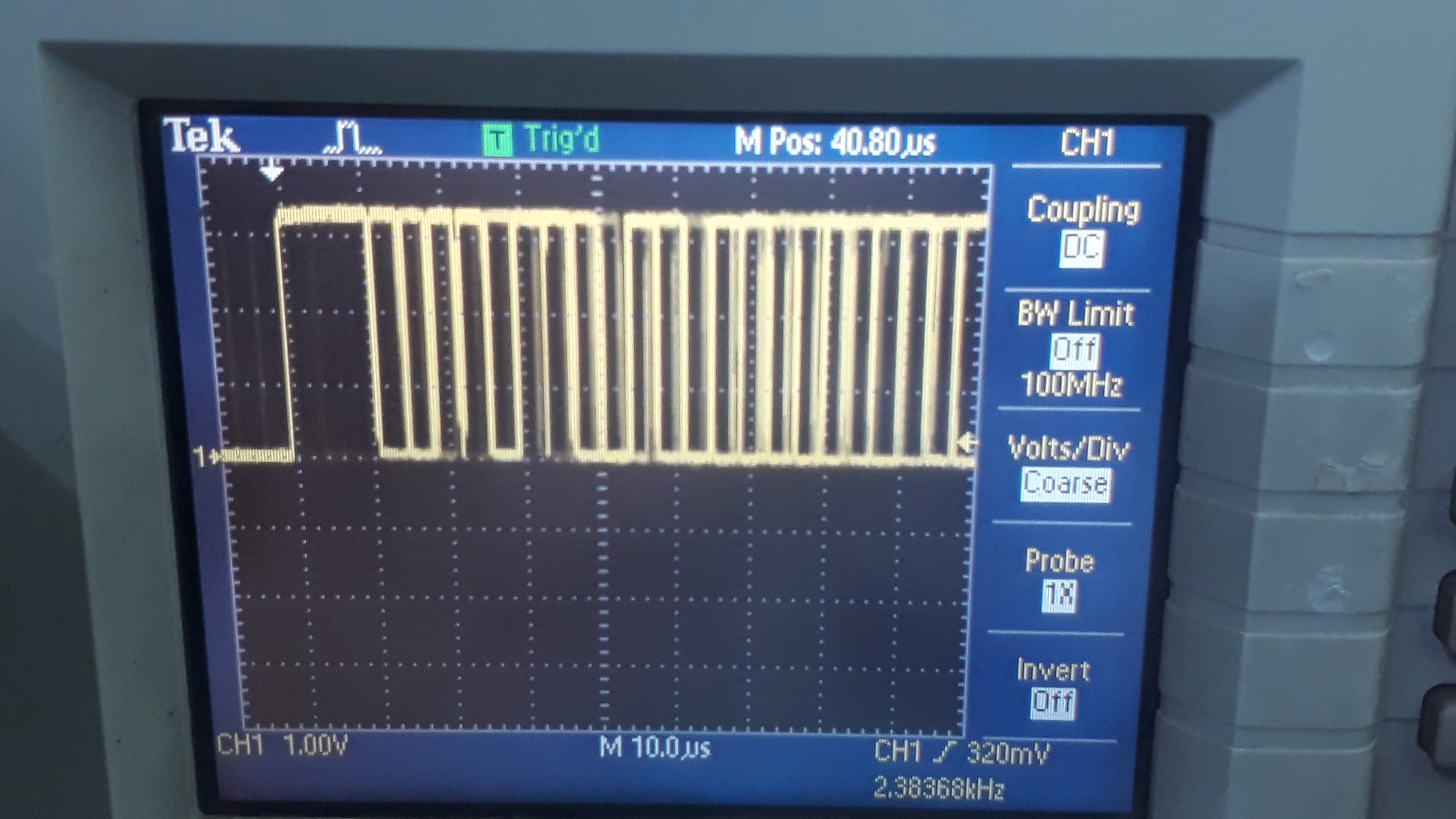
These are the settings, but we get only 15 samples per second(for each channel)

DRDY pin is polled for data ready

We need higher SPS, what can be the solution for it ?

  • Hello Santosh,

    Welcome to the TI E2E Community.

    First, with Fclk=4.2MHz, low speed mode and ClockDiv=1, you should be getting an output data rate for each channel of around 1640sps.  Once the part powers up and the DRDY pin starts toggling, you should be able to measure 1640sps on this pin.  (Note that SYNC pin should be held high.)

    With SCLK=2.56MHz (for best performance SCLK should be closer to 1/2*fCLK=2.1MHz, or limit fSCLK/fCLK to ratios of 1, 1/2, 1/4, 1/8, etc), you should be able to support around 60 channels when using SPI TDM Fixed mode.

    I suspect you are toggling the SYNC pin after each DRDY.    There is a delay in the output data of 129 output conversion cycles after the SYNC pin has been toggled.  Assuming this is what you are doing, the effective output data rate would be reduced to 1640sps/129=13sps.

    The SYNC pin should only be toggled once after the power supplies have stabilized to synchronize all of the ADS1274's in your system.  After that single SYNC pulse, it should be held high and the ADS1274 will continuously convert data.

    Please let me know if this addresses your problem.

    Regards,
    Keith Nicholas
    Precision ADC Applications

  • Hello Keith,

    Thanks for reply.

    after SYNC pin toggled once got following Results at different Fclk.

    Mode: Low speed

    CLKDIV: 1

    Data output format: SPI TDM Fixed

    1)      Fclk - 373 kHz ,SCLK - 328 khz

    144 Samples per Second

     2)     Fclk - 743 kHz ,SCLK - 328 khz

             290 Samples per Second

    3)      Fclk - 1.1 MHZ,SCLK - 1.3 MHZ

             431 Samples per Second

    4)      Fclk - 2.22 MHZ , SCLK - 656 kHz

            746 Samples per Second

     5)    Fclk - 18 MHZ , SCLK - 11 MHZ

           1190 Samples per Second

     6)   Fclk - 21 MHZ , SCLK - 11 MHZ 

          4095 Samples per Second

    Regards,

    Santosh

  • Hi Santosh,

    It looks like you are now getting correct data rates for the first 3 cases.  The output data rate in low speed mode and CLKDIV:1 is Fclk/2560.

    You should be getting higher data rates in cases 4, 5, and 6.  You can confirm by measuring the DRDY frequency. 

    Regards,

    Keith

  • Hello Keith,

    I had confirm with DRDY frequency , it is giving same output as mentioned in
    Can you pleas guide how to improve the sample rate for last 3 cases?

    Regards,

    Santosh

  • Hello Keith,

     Observation i found during Testing 

     ADC Reference  -  1 V

     ADC input voltage - 0.45 V 

     Output Count varies from  0 v to 1.9 v

     Please refer  attached file of ADC output.

     Please guide me to improve our output readings. ADC_Input_Raw_Count.xlsx

    Regards,

    Santosh

  • Hello Santosh,

    Regarding your first question on data rate, as long as Fclk is continuous and stable, the output data rate, and frequency of /DRDY, should be very stable at a frequency of Fclk/2560.

    Possible reasons why /DRDY frequency does not equal Fclk/2560:

    1. Fclk is not stable, or has a high amount of noise.

    2. Fclk is not continuous.

    3. Noise on power supplies or missing bypass capcitors on power supplies.

    Please provide a waveform capture showing Fclk, Sclk, /DRDY, Dout.

    The noise that you see in the readings may be a result of the 'slower' output data rates.  Can you provide the raw ADC readings before conversion to voltage?  

    Please provide a schematic showing the input amplifier and reference circuits.

    Regards,
    Keith

  • Hello Keith,

    Please find the attachment of waveform capture showing Fclk, Sclk, /DRDY, Dout.

    Raw ADC Readings and schematic showing the input amplifier and reference circuits.ADC ckt diag.pdf5808.ADC_Input_Raw_Count.xlsx5808.ADC_Input_Raw_Count.xlsx

  • Hello Santosh,

    I assume your clock is the triangle looking waveform with a frequency of 21.8MHz.  This is likely the cause of the irregular reading rate at the higher frequencies.  This waveform needs to look more like a square wave, and needs to have a peak-to-peak amplitude closer to your IOVDD voltage of 3.3V (it is less than 1Vpp).

    Looking at your schematics, the inputs of the ADC will only accept positive input voltages with respect to ground.  With the ADC negative input tied to ground and a 1V reference, the positive input will only support input voltages from 0V to 1V.  Since the external amplifiers are powered from +/-5V supplies, they could drive the ADC inputs negative, which could cause damage.

    Also, for the reference input, it needs to be driven by a low impedance source similar to the ADC inputs.  Take a look at the ADS1278EVM user's guide for an example of a good ADC input amplifier and reference.

    http://www.ti.com/lit/ug/sbau197a/sbau197a.pdf

    Regards,

    Keith

  • Hello Keith,

    we took care about adc input in hardware which in the of  0v to +1v 

    1st ADC has Volt ref. from ref3125 which is adjust to 1.1 volt and 2nd ADC has Volt ref through adc buffer AD825 

    as  we are not able to improve waveform like square wave at frequency more than  5 MHZ due to some limitations  so we decided to change the mode of adc to get Higher Samples at Low frequency. 

    Mode : High Resolution.

    CLKDIV: 1

    Fclk: 1.1MHZ (image attached)

     ADC_Raw_Count.xlsxSclk: 1.1 MHZ

    Data output format: SPI TDM Fixed

    Samples per Rate is ok as per datasheet,but Adc readings are incorrect.

    please find the attachemet of adc raw readings.

    Regards,

    Aniket

  • Hi Aniket,

    The clock waveform now looks correct.

    You are using two 4 channel ADC's, so a single transfer will consist of 8x24=192 bits.  SCLK will need to be at least 1/2*Fclk, or 550kHz.  However, keeping SCLK at the same frequency as Fclk will be best to transfer the data.

    Please try to capture /DRDY, SCLK, Dout using a 4 channel scope, or trigger on /DRDY and capture both SCLK and DOUT using a dual channel scope with external trigger.

    Regards,
    Keith

  • Hi Keith,

    Mode : High Resolution.

    CLKDIV: 1

    Fclk: 1.1MHZ (image attached)

    Sclk: 1.1 MHZ

    Please find the waveform of DOUT and SCLK.

    Channel 1 - SCLK.

    Channel 2 - DOUT.

    Regards,

    Aniket

  • Hello Aniket,

    Please capture /DRDY and SCLK.

    Channel 1 - SCLK.

    Channel 2 - /DRDY

    Please provide waveform captures with time division of 250uS/div and 1uS/div.

    The /DRDY should be a fixed frequency of Fclk/512 = 1.1MHz/5212 = 2.15ksps (Fclk=1.1MHz, high-resolution, CLKDIV=1).  Your above waveforms apear to show a data rate of about 1ksps, which indicates your MCU is not reading the data back fast enough.

    Regards,
    Keith

  • Hello Keith,

    Please find attachment of  waveform captures with time division of 250uS/div and 1uS/div.

    Channel 1 - SCLK.

    Channel 2 - /DRDY

    one more observation during testing is if fSCLK is greater than fCLK ADC Readings are correct compare to fSCLK/fCLK to ratios of 1, 1/2, 1/4, 1/8

    Regards,

    Aniket

  • Hi Aniket,

    Conversion results are ready on every falling edge of /DRDY.  From the above scope capture, you are only retrieving every other reading.  I circled all of the edges where conversion results can be clocked out of the ADC.

    Also, SCLK appears to be going hi-impedance between readings.  The SCLK must be driven high or low and not allowed to float for proper operation of the ADC.  After clocking the last bit out of the ADC, it would be best to leave SCLK in the low state.

    One other comment.  Since you are reading data from 2 ADS1274 devices, the converters need to be synchronized to each other for proper operation.  You can do this by driving the /SYNC pin low and then high after the power supplies have stabilized.  Please refer to page 27 of the datasheet (SYNCHRONIZATION) and Figure 73 for details.

    Regards,
    Keith

  • Hi Keith,

    Thanks for solution.

    Regards,

    Aniket

  • This error is caused by a PC buffer overflow. The PC buffer is the buffer that exists on a computer between the DAQ hardware and LabVIEW's application memory. It is written to continuously by hardware, but is only periodically read from by LabVIEW. This can often lead to a mismatch in read rates. Typically, data is overwritten in the DAQmx PC Buffer because either the read rate is slower than the sample rate, or the DAQmx PC Buffer is too small to hold the data required by the DAQmx task. shareit app vidmate apk