This thread has been locked.

If you have a related question, please click the "Ask a related question" button in the top right corner. The newly created question will be automatically linked to this question.

ADS8332: Can not read Data / Just get "FFFF"

Part Number: ADS8332

Hello everyone,

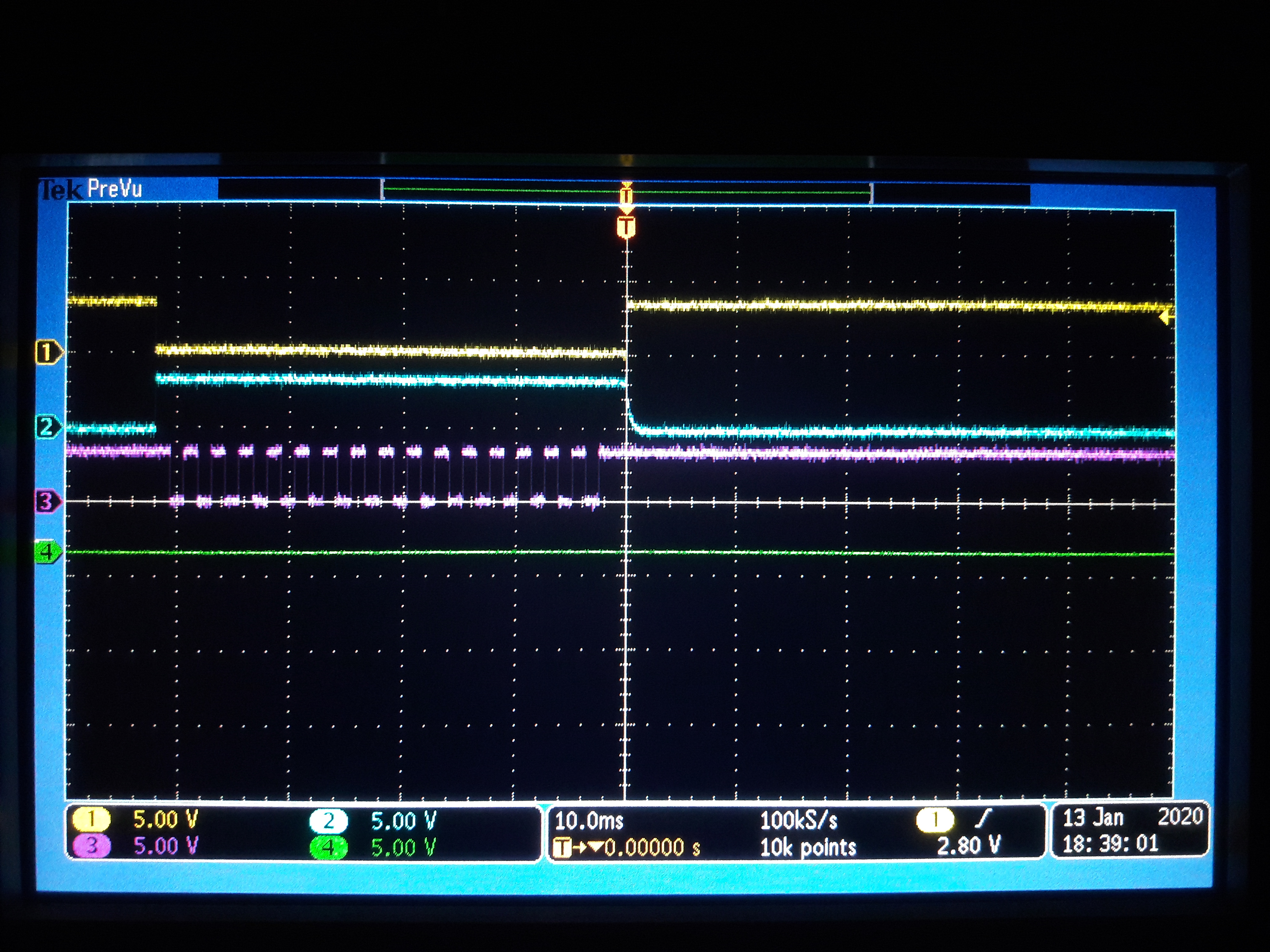
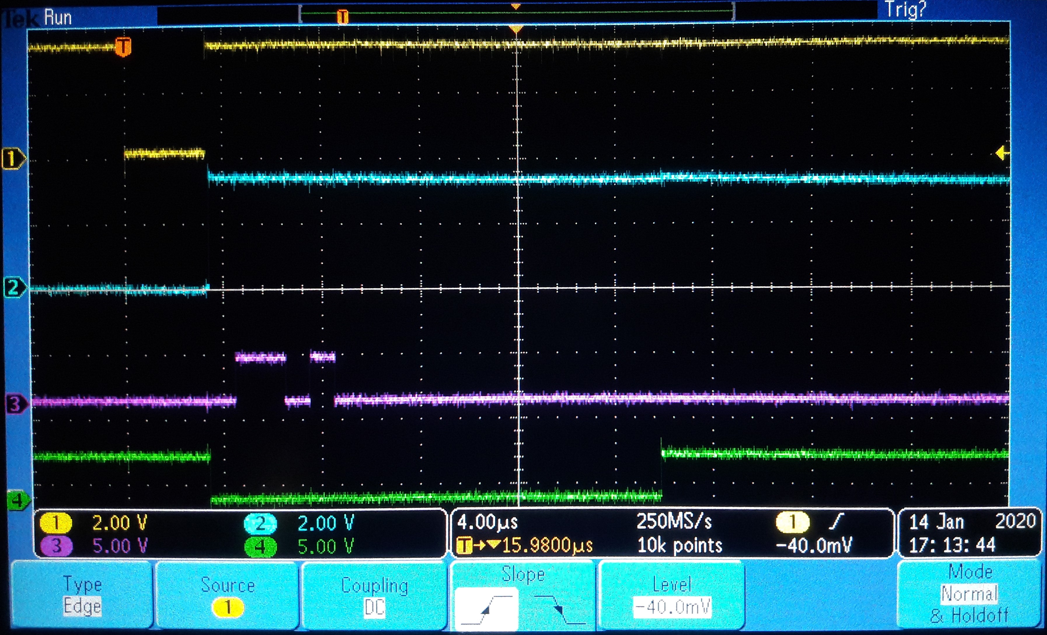
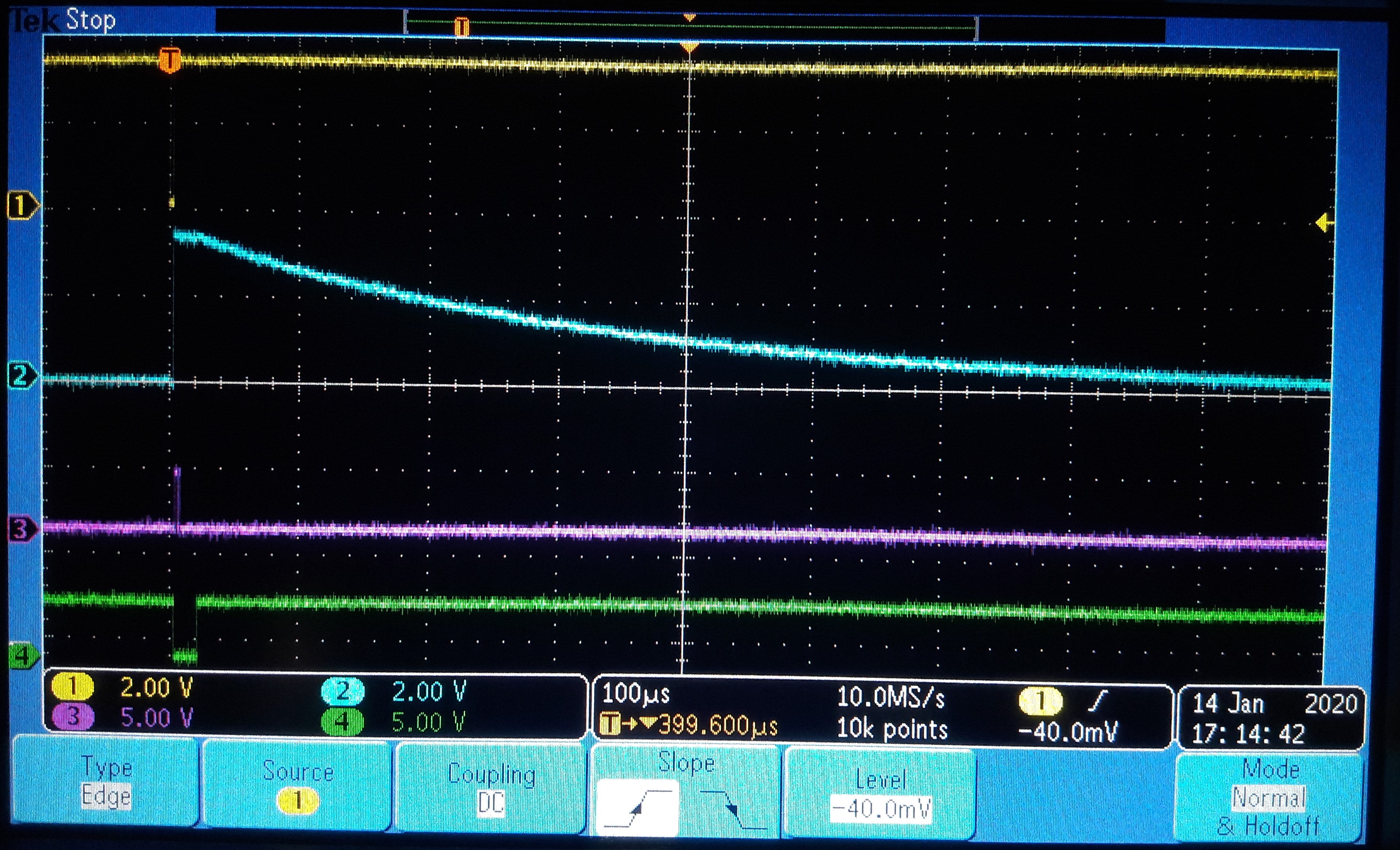
I'm just getting started with the ADS8332. First, I try to read data from a single channel to proof my ADC is working, but even this shows me just the maximum value (65535).

I work with the ESP32 mikrocontroller and got this code so far:

#include <Arduino.h>
#include <SPI.h>

#define SS 5
#define SCLK_Pin 18
#define MOSI 23
#define MISO 19
#define Reset 22
#define CONVST 17
static const int spiClk = 40 * 10^6;  //40MHz

int data;

void setup() {
  Serial.begin(115200);

  pinMode(SS, OUTPUT);
  digitalWrite(SS, HIGH);
  //pinMode(CONVST, OUTPUT);
  //digitalWrite(CONVST, HIGH);
  SPISettings(spiClk, MSBFIRST, SPI_MODE2);
  SPI.begin(SCLK_Pin, MISO, MOSI, SS);
  
  digitalWrite(SS,LOW);
  SPI.transfer16(0xE07D); //0b1110000001111101
  Serial.println("Uploaded CFR");
  SPI.transfer16(0x7000); //0b0111000000000000
  Serial.println("Selected Channel 7");
  Serial.println(SPI.transfer16(0XC000)); //try to get CFR back. ->Also don't works
  digitalWrite(SS, HIGH);
}

void loop() {
  digitalWrite(SS, LOW),
  // digitalWrite(CONVST, LOW);
  // digitalWrite(CONVST, HIGH);
  // SPI.transfer16(0xD000);
  // data = SPI.transfer16(0);
  data = SPI.transfer16(0xD000);
  digitalWrite(SS, HIGH);
  Serial.println(data);
  delay(1000);
}

The outcommented lines are attempts the get it work.

Thanks in Advance!

  • Hello Lasse,

    Welcome to the TI E2E community.

    In order to debug, I suggest not writing to the configuration register and using the default reset value 0xFFF.  In this mode, the ADC will use the internal conversion clock and you can then replicate the timing waveforms shown in Figure 1 of the datasheet.

    Please capture the waveforms /CONVST, /CS, SCLK, and SDO with a 4 channel scope and post a copy here.

    Regards,
    Keith Nicholas
    Precision ADC Applications

  • Hi Keith,

    a change to default settings also gets me just the maximum value.

    And this are the captured digital signals (running with the code above):

    1. CS
    2. SCLK
    3. SDO
    4. CONVST

    Thank you and best Regards!

  • Hello Lasse,

    I assume the waveforms are as follows:

    1. /CS

    2. SDO

    3. SCLK

    4. /CONVST

    The /CONVST line is not toggling and low during the entire frame.  The /CONVST needs to toggle low and then high to start a conversion.  After the maximum conversion time of 1.65uS (when using the internal conversion clock), you can then take /CS low and clock the data out of the device.

    Hopefully pulsing the /CONVST low will get the device working correctly.  The MSB is launched when /CS goes low, and then on each of the following SCLK falling edges.  Since SCLK is high when /CS is pulled low, the first falling edge of SCLK will shift the next bit out onto SDO.  Your MCU in this case will need to capture data on the SCLK falling edge in order to capture the MSB correctly.

    Regards,
    Keith


  • Hi Keith,

    sorry, you are right, I confused the Ports.

    Now, I toggle the CONVST low for 2us and then I toggle the CS low while I try to read the value. But the SDO channel looks weird. Seems more like a discharging capacitor instead of a digital signal. (thats why I'm getting the max value everytime) My SDO line is connectet to pin 13.

    Is it right that the SDO signal looks like that?

    1. COVST
    2. SDO
    3. SDI
    4. CS

    or in an overview:

    Do you maybe have any example codes for this kind of ADC which I can compare to mine?

    Thank you and regards,

    Lasse

  • Hi Lasse,

    It appears that the ADC is not properly powered up or is being held in reset condition.  (Below pin numbers for TSSOP package.)

    1. Please measure voltage on pin 17, VA supply pin.  Verify it is in the range from 2.7V to 5.5V.

    2. Please measure voltage on pin 16, VBD supply pin.  Verify it is in the range from 1.65V to VA+0.2V.

    3. Verify /RESET pin 8 is high level, equal to VGD supply voltage.  (I assume 3.3V based on your scope pictures.)

    4.  Verify REF+ pin 18 is in the range of 1.2V to 2.525V.

    Regards,
    Keith

  • Hi Keith,

    my reset pin was low all the time. Thank you for your advice!

    My Ref+ is the same as VA. Both are about 3.6V. Is this bad? Because it seems like I get correct values.

    Regards,

    Lasse

  • Hi Lasse,

    Glad to hear that the device is now working!

    The ADC will function correctly, but you are outside of the recommended conditions to meet the published specifications.  I would suggest using a 2.5V or 3.0V reference value and reducing the VA voltage to 3.3V for best performance.

    Regards,
    Keith