This thread has been locked.

If you have a related question, please click the "Ask a related question" button in the top right corner. The newly created question will be automatically linked to this question.

ADC12J1600EVM: using pin headers to program ADC and LMK with SPI instead of FTDI + GUI

Part Number: ADC12J1600EVM

Hi,

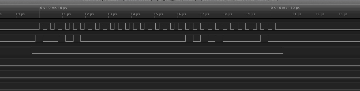
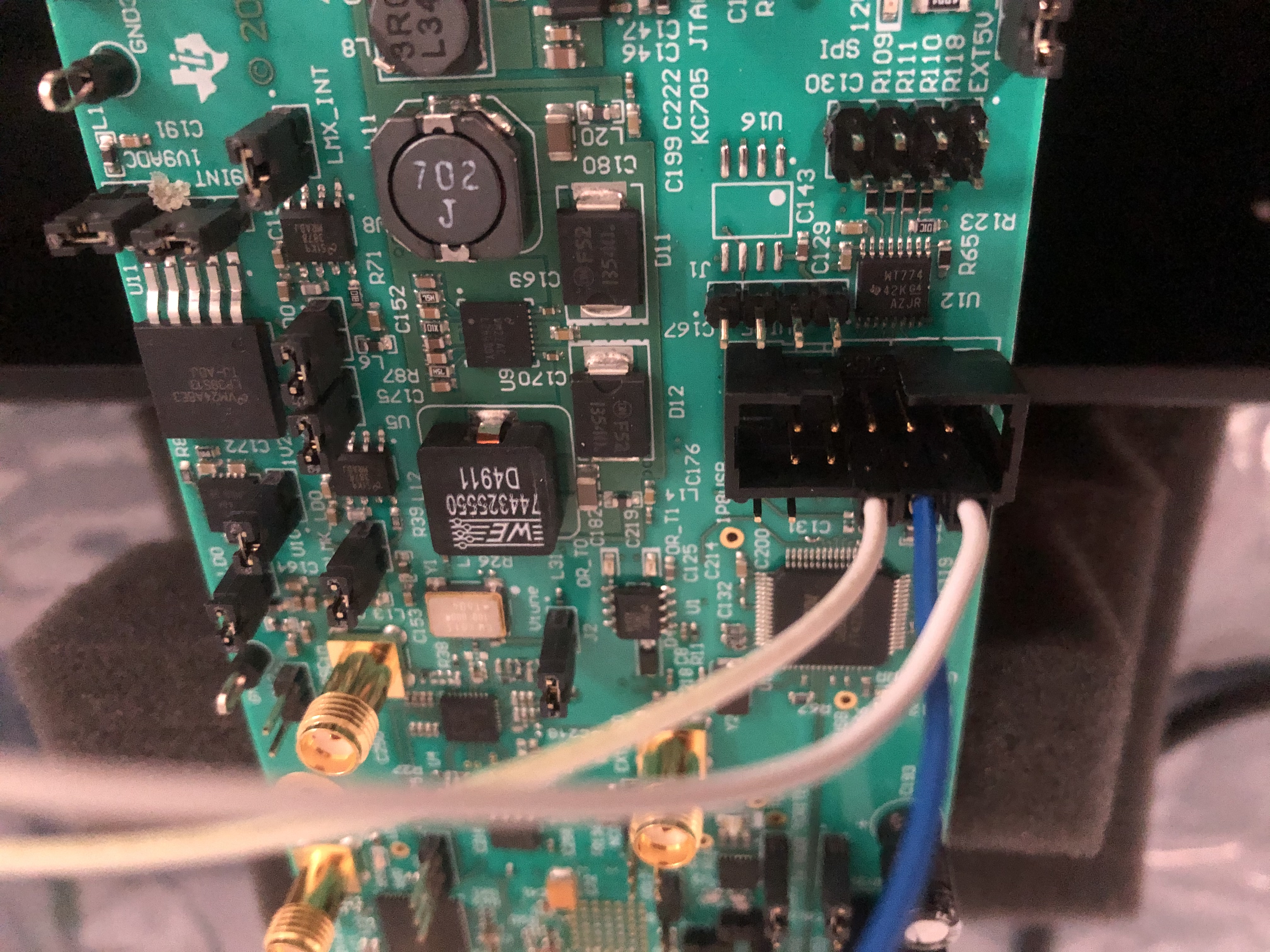
I want to use the pin headers on the board to connect an FPGA board and program the devices externally using SPI over the connectors

instead of using the FTDI chip apart from connecting some wires , do i need to mod the board in anyway?

also have wired up the correct pins on the header for LMK SPI?

Regards,

Charles

  • Charles,

    For the ADC, you need to remove R118, R110, R111, and R109. These are located on the top side between U12 and the connector.

    For the LMK and TRF3765, you need to remove R68, R113, R114 and R115. These do not have silkscreen but are identified in the attached picture.  

    Your connections shown look correct as far as I can tell.

    Regards,

    Jim

    R115, R68, R114 and R113.pptx

  • Hi Jim,

    so i have removed the resistors as you said and connected up both headers i have, my FPGA is writing all the registers in the same order as the GUI (using the config files as a guide) and also each SPI interface is copying the pattern files also supplied with the GUI

    Nothing is happening.

    the LMK/TRF header i'm using 3.3v volt pins from FPGA

    the ADC i'm using 1.9v pins (actually its 3.3v out of the FPGA) but i'm going through a level shifter.

    I'm a missing anything?

    i have a logic analyser which i used to capture the FTDI transfers (we have 2 ADC boards) and i'm pretty sure the protocol is the same.

    one thing i noticed is if i probe the other side of the 12.4k resistors with logic analyser its seems to not pick up the signals properly, they seem like quite large resistors could that be an issue?

    Regards,

    Charles

    P.S i got all the jesd stuff from other thread working!

  • Hi Jim

    so am able to talk to the LMK04028 ok

    i'm not seeing any clocks coming being activated though would that be the TRF3765

    Regards,

    Charles

  • Charles,

    The SPI for the TRF3765 works differentially than the other parts. Is your interface following the protocol as shown in the attached document?

    Regards,

    Jim

     TRF3765 SPI.pptx

  • Hi Jim,

    i don't think your right there 

    it seems to be the same to me the latch enable is basically just the slave select.

    below is a capture from FTDI to TRF3765  thsi is register 9 being written:

    i'm running the SPI at 20Mhz which is its top rated , i noticed the FTDI runs at a slower frequency about 3.125Mhz

    so might try at a lower frequency

    Regards,

    Charles

  • Charles,

    Not sure what you meant by "I don't think you are right there". What Is sent was directly from the data sheet. Are you saying you are following this protocol and my guess at your problem was incorrect? If so, have you tried running your SPI at a lower rate? Did this help?

    Regards,

    Jim 

  • Hi Jim,

    so i ran at 10Mhz and still the same result i can write/read the lmk ok , but the TRF and ADC seem unresponsive

    i'm following the datasheets for all the devices , plain and simple it should work buts not working

    the ADC and LMK have exactly the same protocol and yet one works and one doesn't (same code for both)

    am stumped 

    Regards,

    Charles

  • Charles,

    From your last response, I cannot tell which part you are having success with. I am guessing the ADC only. The LMK defaults to 3 wire SPI mode at power up. We have to change this 4 wire SPI mode to get a valid read back with our GUI. For your other issues, You should just be able to repeat what the FTDI and GUI does. Are the voltage levels correct?

    Regards,

    Jim

  • Hi Jim,

    no i said i can talk to the LMK

    but not the ADC or TRF

    the voltages are 1.9v for the ADC header 

    And 3.3v for the LMK/TRF

    I've also tried altering the slew rate, too no effect.

    just tried running the interface at 6.25 Mhz but again no joy.

    Regards,

    Charles

  • Charles,

    For the ADC, make sure you are sending CS low when SCLK is low. I don’t think the ADC will respond if CS goes low when SCLK is high.


    The detailed SPI spec from the digital team is attached. The drawing in the ADC12Jxx00 datasheet doesn’t show this well/properly.

    Regards,

    Jim

     SPI Timing diagrams.docx

  • Hi Jim,

    so i'm copying the protocol of the FTDI exactly now for all 3 devices i still get a response for the LMK,  but not the ADC or TRF.

    i don't what else to do 

    the attached shows my setup which i'm pretty sure is correct does the FPGA have to drive the pins at any kind of particular current rating?

    Left of the picture

    TRF/LMK header

    - top blue - TRF strobe

    - orange - LMK Chip select

    - bottom blue - DATA IO

    - grey - clock

    Right of picture

    ADC header

    - top orange - clock

    - grey - data to ADC

    - yellow - data from ADC

    - bottom blue - chip select

    also the you can see removed the resistors as well for connecting the FTDI (wires on left slightly obscured by grey wire but have been removed)

  • Charles,

    I did not design this board and maybe there is an error with the schematic. Can you probe at the pins of both the ADC and TRF devices and verify the signals are toggling and at the correct voltage level? There is no current requirement that I know of for these pins.

    Regards,

    Jim

  • Charles,

    Here is another test you can try. With R118, R110, R111 and R109 removed, solder wires between the pads of these resistors that are connected to U12 and the other end of these wires connect to the SPI connector. Then use the GUI to write to the ADC. If you can communicate with the ADC, then the connections between the SPI connector and the ADC is correct and the issue is with your FPGA. If it doesn't work, there is something wrong with the schematic.

    Regards,

    Jim


  • Hi Jim,

    I only need to program the LMK04828 for there to be a clock coming into the FPGA correct?

    i use the same configuration as the GUI but its does not give me any clocks , is there some reset or something i'm missing?

    even though i seemingly can write/read registers from the LMK (e.g if i write X"0A" to the register i get X"0A" back) , it still does not give me a clock.

    i still cannot talk to the ADC either, i'm about ready to give up i believe i'm 99% sure i'm doing everything correctly.

    there has to be some information that i don't have, does the FTDI only program up the registers for 3 (i'm aware its also programs the temp chip, but i don't care about that) devices or does it do other things as well?

    if i write a register i should be able to immediately read it back and get the data i just wrote, correct?

    do i need to tri-state any of the signals? i'm only tri-stating the lmk-sdio at the moment.

    have you had any issues with talking to these devices before on these boards? 

    Regards,

    Charles

  • Charles,

    After powering up the ADC, the GUI allows me to write and read registers of the ADC without programing the LMK or TRF devices. I checked the SPI connector and the traces Ohm out properly to the ADC. Did you try any of the tests I suggested? I cannot tell from your reply.

    I would focus on only doing writes to the ADC. With the EVM powered up, the current usage is at 0.966A. After writing a "3" to register 0x02 this drops to 0.520A (power down mode). I would suggest you try this test.

    Regarding the LMK, the TRF3765 must be programed to provide a clock to the LMK. This is probably why you are not getting any clock outputs from the LMK.

    The FTDI only programs the three parts.

    If you write to an ADC register you should be able to read back the results immediately.

    You do not need to tri-state any signals.

    We have not had any issues talking to these parts.

    Regards,

    Jim