This thread has been locked.

If you have a related question, please click the "Ask a related question" button in the top right corner. The newly created question will be automatically linked to this question.

TSW14J56EVM: TSW14J56EVM

Part Number: TSW14J56EVM

Hello,

I have some questions concerning working with  TSW14J56EVM  board connecting to ADS54J40EVM board.

1. I want to sample only one "frame" of 1 Giga Pixels (using all the memory of one connected ADC) by using one shot trigger connecting to 

    J13 ( TRIG IN) on the board and be able to read all the 1 GPixels. (Working like a single trigger Scope).

2. Using the board normally (no outside triggers) I can only read 65000 points. The memory is 1 G points per ADC. How can I read them all.

3. Is it possible to give a sequence of triggers let say - 100000 - 10 us apart  and then read the 1 Giga points. ( 10000 points at 1 Ghz sample rate for an interval of 10 us for 1 Sec.)

Regards,

Giora

  • Giora,

    For #1, see the trigger section of the HSDC Pro User's Guide which I have attached.

    For #2, in HSDC Pro GUI, go to the "Data Capture Options' tab then select "Capture Option". Here you need to change the default value of 65536 to the size you want. This determines the memory size used for captures.

    For #3, there is not an option available to do this using the trigger feature. There are some features with the automation functions that may allow this. Information regarding this can be found in the following location:

    C:\Program Files(86)\Texas Instruments\High Speed Data Converter Pro\HSDCPro Automation DLL

    Regards,

    Jim 

    slwu087d.zip

  • Jim,

    Thanks.

    Giora

  • Hi Jim,

    One other question concerning the ADC board - ADS54J40EVM:

    1. Does the input transformer circuit is matched to 50 ohm source input?

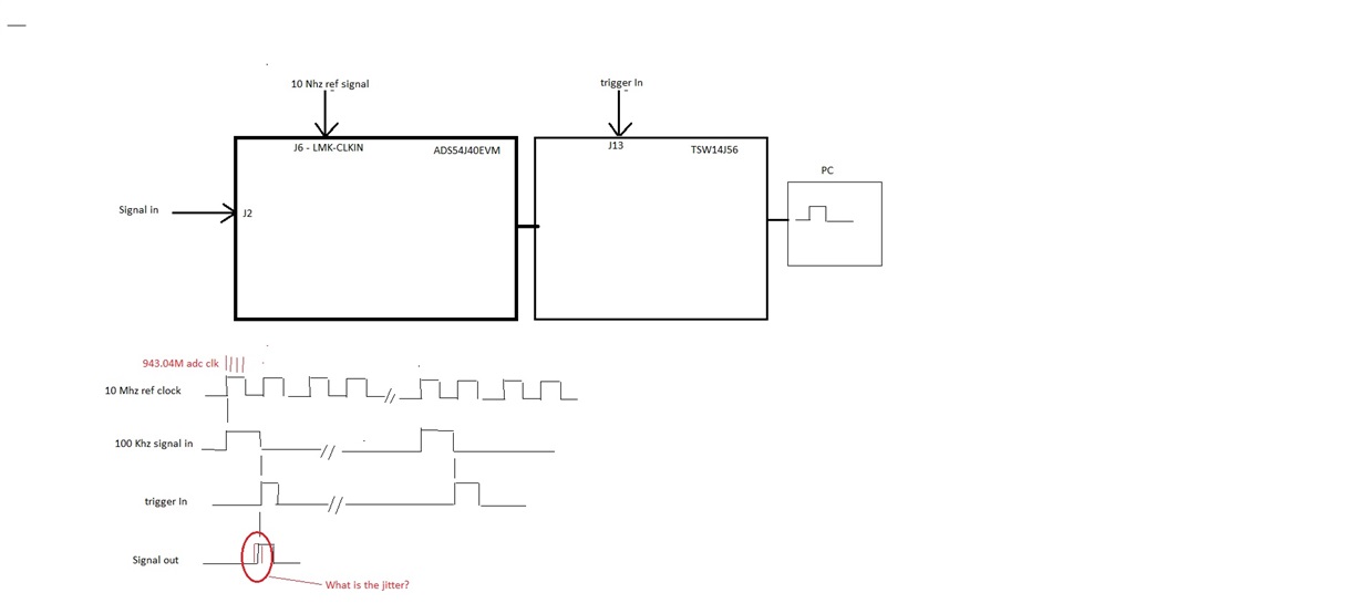
    2. We want to synchronize the ADC with 10 Mhz signal source. When doing it is the signal-in, that also synchronized to the 10 Mhz ref clock

        will be synchronize to the ADC clock of 943.04 Mhz. (see attached drawing)

    3. When using the trigger in ( J13 on TSW14J56) what will be the jitter of the signal out (the sampled signal in by the ADC) between trigger in pulses)

  • Giora,

    1. Yes, 50 Ohms.

    2. Is this a question? I cannot tell.

    3. See the attached documents4137.TSW14j56_MC firmware design document.pdf which explains how the trigger function works. This is a logic output from an Altera 5AGZME1EZH29C3N Arria V device. You would have to either consult the data sheet for this info or measure the jitter yourself. This is something we have not measured.

    Regards,

    Jim

    TSW14J56revD Trigger.docx

  • Jim,

    Thanks.

    In question 3 I meant:

    If the signal input to the adc board (J2) and the trigger input to J13 (EXT _TRIG) on TSW15J56 are all synchronized to the 10 Mhz ref clock (J6 on adc board)

    Giving a single shot trigger on the EXT_TRIG and capture the signal input - let say that the signal input is a rectangular pulse - and on the PC GUI

    the pulse is started at clock 1000.

    Now a second trigger is given and we capture again the signal input.( It is the same signal as the first one with the same relations between the signal input the trigger and the 10 Mhz ref clock.) My question is the captured rectangular pulse will also start at clock 1000 on the PC GUI or will it has a jitter?

    Regards,

    Giora

  • Giora,

    If the trigger is synchronized to the 10MHz reference and an integer factor of the local multi-frame clock (LMFC), then the start should be the same for each capture.

    Regards,

    Jim

  • Jin,

    Thanks.

    How to make the 10 Mhz ref clock an integer factor of the LMFC clock?

    Regards,

    Giora

  • Giora,

    Not the 10MHz reference, the trigger must meet this requirement. The LMFC will already be synchronized by the 10MHz. LMFC calculation attached.

    Regards,

    Jim

    bit rate calculation.docx

  • Jim,

    Thanks.

    Regards,

    Giora

  • Hi Jim,

    Another question regarding the ADS54J40EVM board.

    We are using the VCO 122.88 Mhz as the source to get the  ADC clock.

    The configuration allow us to chose the 943.04 Mhz.

    Can we change it say to 960 Mhz?

  • Giora,

    The issue is not only with the VCXO but the LMK device. The LMK04828 has two internal PLL's that will not allow this range. You have to options to get this to work:

    1. Change the LMK04828 to a LMK04826 and change the VCXO to 120MHz.

    2. Use the LMK04828 in clock distribution mode and provide an external 960MHz.

    Regards,

    Jim 

  • Jim,

    Thanks.

    Regards,

    Giora