


Part Number: ADS8668EVM-PDK
Hello,
I am currently using the ADS8668EVM-PDK and have gone through the user's manual instruction to include the use of the built-in GUI that comes with the capture card (SDCC). As of now, I am using the EVM board stand-alone and without the capture card. When issuing a write command to the program register 03h Data: 41h, I am doing so in SPI Mode 1 (Low Polarity, Falling Edge) and based on the response of the ADS8668 it recognizes this command. However, the expected response data which consists of the echoed data bits is returned in SPI Mode 0 (Low Polarity, Rising Edge). With the return data having a phase shift, I decided to try the write command as SPI Mode 0 to then see how the response is read. Doing this, the IC has no response, because it is expecting SPI Mode 1. I have provided a screenshot of the results below...
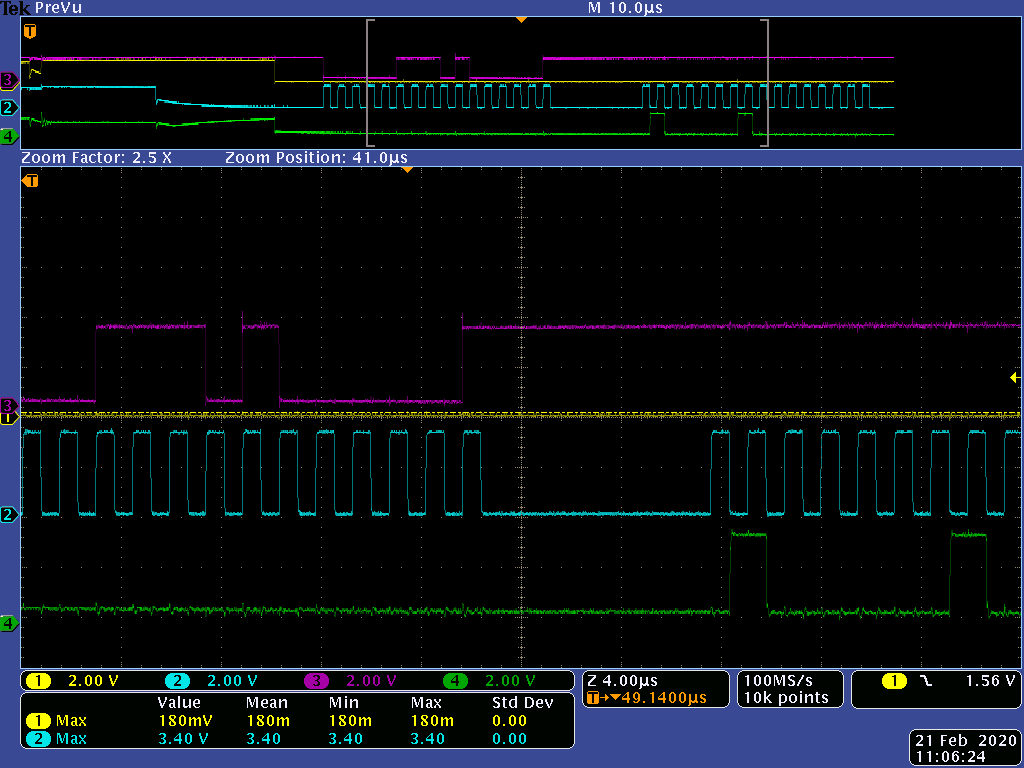
Is it expected that the IC's response would be in SPI Mode 0? There was an initial thought that maybe the IC was responding Asynchronously and arbitrary to the clock and therefore appeared to have a phase shift. However, when playing with parameters and delaying the response bites, the IC still doesn't respond until the clock initiates. Nonetheless, the data is still the same regardless of latency between the 16th and 17th clock pulses. It doesn't make sense that you would issue a command in one SPI mode and then have to receive in a different one. Any and all help is greatly appreciated!
Thank You,
Dustin


