This thread has been locked.

If you have a related question, please click the "Ask a related question" button in the top right corner. The newly created question will be automatically linked to this question.

ADS7950: Data out is always 0x7FFF

Part Number: ADS7950

MCU is STM32L4R5ZI No operating system - bare metal

Manipulating GPIOs directly, (not using SPI block in the ST Micro MCU on our board)

  • REFP Analog reference voltage input 2.5V
  • CH0: 0.229V
  • CH1: 0.341V
  • CH2: 0.356V
  • CH3: 2.440V

dataIn:

  • #define ADC_DATA_IN_CH0_FWD_PWR2 0x1800
  • #define ADC_DATA_IN_CH1_FWD_PWR 0x1880
  • #define ADC_DATA_IN_CH2_REV_PWR 0x1900
  • #define ADC_DATA_IN_CH3_ALC_OUT 0x1980

dataOut:

Constant 0x7FFF 

Sending 4 each for each channel every 100ms, so the pipeline is flushed completely for each channel before moving on

From the datasheet it looks like config is entirely contained in every request, but did I miss something?

Is there a one time init sequence?

Or something on the hardware side during reset?

fromtop_cs_sclk_sdo_sdi_2us..jpg

rf_power_measurement_schematic.png

  • Above is a summary of a post to customer service forum:

    https://ticsc.service-now.com/csm/?sys_id=3b3dac6c1b970410d355ca217e4bcb2c&id=csm_ticket&table=sn_customerservice_case 

    More pictures and detail of code snippets available there

  • Hello Andy,

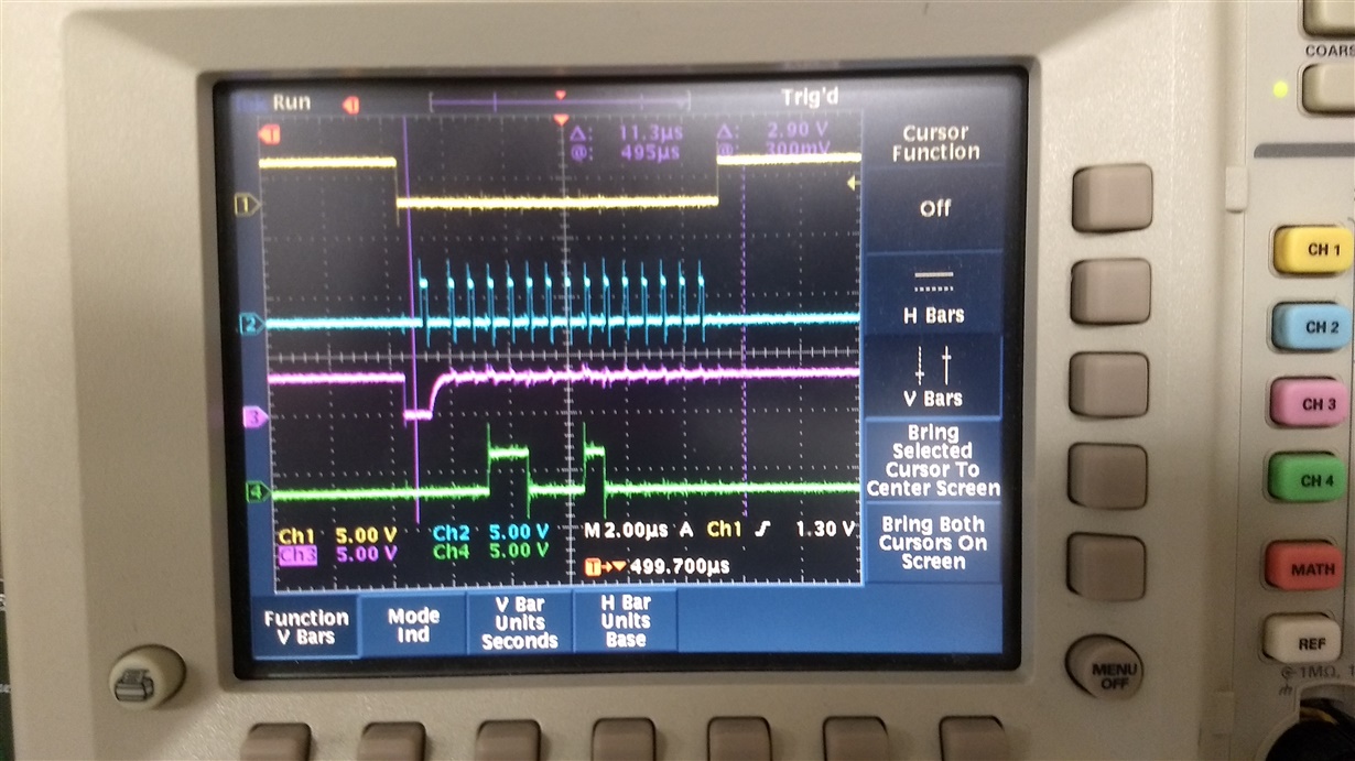
    From your scope shot, it does not seem you have enough SCLKs. this device needs 16 SCLKs, note that the data outputted on the falling edge of SCLK, currently you only have 15 falling edges. The CS signal should not be brought up before 16 SCLKs.

    The commands you shared do seem correct.

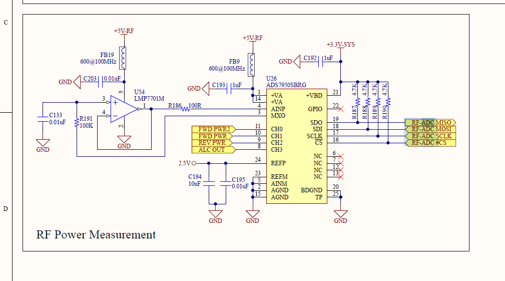
    Looking at your schematic, it looks good. The 100k resistor and .01uF capacitor at the MXO to the buffer input creates a very low cut off frequency, from the looks of it, the analog inputs seems to be all DC. Is this why the RC was added to the buffer?

    Regards,

    Cynthia

  • Hello Cynthia--

    Oof, I can't believe I didn't notice the short clock - thanks.

    Now I'm seeing some action from the chip, but it's still not acting as described in the datasheet.

    I have debug output that shows data in and data out.  I would expect that when I change channel, it will take a few more transactions before I start seeing values coming back for that channel.  To make this easier to see, and also to insure that the voltage input from the RF section has time to stabilize, I now send queries at 10ms interval, sending in groups of 4 per channel, saving the result on the fourth try for each channel.  I would expect by then that the result returned should be for the same channel I am asking for.

    What I see instead is something like this:

    (previously asked for chan 0 4 times)

    ask(chan 1)  1st time, top 4 MSBs = 1

    ask(chan 1)  2nd time, top 4 MSBs = 6

    ask(chan 1)  3rd time, top 4 MSBs = 0

    ask(chan 1)  4th time, top 4 MSBs = 6

    (Don't save this time because the upper bits seem to indicate an error)

    ask(chan 2)  1st time, top 4 MSBs = 6

    ask(chan 2)  2nd time, top 4 MSBs = 0

    ask(chan 2)  3rd time, top 4 MSBs = 1

    ask(chan 2)  4th time, top 4 MSBs = 1

    [Save a valid value for channel 1?)

    A snippet of 3 complete cycles of debug output follow

    (Is there a way to attach files in this foum or does everything have to be pasted into this texr?

    Thanks for your quick response,

    --Andy

    getADC( 0x0) dataIn = 0x1800 dataOut = 0x177f dataOut(4 MSBs) = 0x1
    getADC( 0x0) dataIn = 0x1800 dataOut = 0x677f dataOut(4 MSBs) = 0x6
    getADC( 0x0) dataIn = 0x1800 dataOut = 0x7b60 dataOut(4 MSBs) = 0x7
    getADC( 0x4) dataIn = 0x1800 dataOut = 0x6b60 dataOut(4 MSBs) = 0x6
    getADC( 0x1) dataIn = 0x1880 dataOut = 0xb60 dataOut(4 MSBs) = 0x0
    getADC( 0x1) dataIn = 0x1880 dataOut = 0x6360 dataOut(4 MSBs) = 0x6
    getADC( 0x1) dataIn = 0x1880 dataOut = 0x7f12 dataOut(4 MSBs) = 0x7
    getADC( 0x5) dataIn = 0x1880 dataOut = 0x7f12 dataOut(4 MSBs) = 0x7
    getADC( 0x2) dataIn = 0x1900 dataOut = 0x92 dataOut(4 MSBs) = 0x0
    getADC( 0x2) dataIn = 0x1900 dataOut = 0x92 dataOut(4 MSBs) = 0x0
    getADC( 0x2) dataIn = 0x1900 dataOut = 0x1111 dataOut(4 MSBs) = 0x1
    getADC( 0x6) dataIn = 0x1900 dataOut = 0x1111 dataOut(4 MSBs) = 0x1
    >>> saveValidData[ 1 ] = 273
    getADC( 0x3) dataIn = 0x1980 dataOut = 0x6111 dataOut(4 MSBs) = 0x6
    getADC( 0x3) dataIn = 0x1980 dataOut = 0x6111 dataOut(4 MSBs) = 0x6
    getADC( 0x3) dataIn = 0x1980 dataOut = 0x1b7f dataOut(4 MSBs) = 0x1
    getADC( 0x7) dataIn = 0x1980 dataOut = 0x677f dataOut(4 MSBs) = 0x6
    getADC( 0x0) dataIn = 0x1800 dataOut = 0x677f dataOut(4 MSBs) = 0x6
    getADC( 0x0) dataIn = 0x1800 dataOut = 0x77f dataOut(4 MSBs) = 0x0
    getADC( 0x0) dataIn = 0x1800 dataOut = 0x7b60 dataOut(4 MSBs) = 0x7
    getADC( 0x4) dataIn = 0x1800 dataOut = 0xb60 dataOut(4 MSBs) = 0x0
    >>> saveValidData[ 0 ] = 2912
    getADC( 0x1) dataIn = 0x1880 dataOut = 0x7360 dataOut(4 MSBs) = 0x7
    getADC( 0x1) dataIn = 0x1880 dataOut = 0x7360 dataOut(4 MSBs) = 0x7
    getADC( 0x1) dataIn = 0x1880 dataOut = 0x7f12 dataOut(4 MSBs) = 0x7
    getADC( 0x5) dataIn = 0x1880 dataOut = 0x7f12 dataOut(4 MSBs) = 0x7
    getADC( 0x2) dataIn = 0x1900 dataOut = 0x1f12 dataOut(4 MSBs) = 0x1
    getADC( 0x2) dataIn = 0x1900 dataOut = 0x92 dataOut(4 MSBs) = 0x0
    getADC( 0x2) dataIn = 0x1900 dataOut = 0x6111 dataOut(4 MSBs) = 0x6
    getADC( 0x6) dataIn = 0x1900 dataOut = 0x6111 dataOut(4 MSBs) = 0x6
    getADC( 0x3) dataIn = 0x1980 dataOut = 0x1111 dataOut(4 MSBs) = 0x1
    getADC( 0x3) dataIn = 0x1980 dataOut = 0x6111 dataOut(4 MSBs) = 0x6
    getADC( 0x3) dataIn = 0x1980 dataOut = 0x7b7f dataOut(4 MSBs) = 0x7
    getADC( 0x7) dataIn = 0x1980 dataOut = 0x7b7f dataOut(4 MSBs) = 0x7
    getADC( 0x0) dataIn = 0x1800 dataOut = 0x677f dataOut(4 MSBs) = 0x6
    getADC( 0x0) dataIn = 0x1800 dataOut = 0x677f dataOut(4 MSBs) = 0x6
    getADC( 0x0) dataIn = 0x1800 dataOut = 0x1760 dataOut(4 MSBs) = 0x1
    getADC( 0x4) dataIn = 0x1800 dataOut = 0x6b60 dataOut(4 MSBs) = 0x6
    getADC( 0x1) dataIn = 0x1880 dataOut = 0x6b60 dataOut(4 MSBs) = 0x6
    getADC( 0x1) dataIn = 0x1880 dataOut = 0x1360 dataOut(4 MSBs) = 0x1
    getADC( 0x1) dataIn = 0x1880 dataOut = 0x7f12 dataOut(4 MSBs) = 0x7
    getADC( 0x5) dataIn = 0x1880 dataOut = 0x1092 dataOut(4 MSBs) = 0x1
    >>> saveValidData[ 1 ] = 146
    getADC( 0x2) dataIn = 0x1900 dataOut = 0x92 dataOut(4 MSBs) = 0x0
    getADC( 0x2) dataIn = 0x1900 dataOut = 0x1092 dataOut(4 MSBs) = 0x1
    getADC( 0x2) dataIn = 0x1900 dataOut = 0x1111 dataOut(4 MSBs) = 0x1
    getADC( 0x6) dataIn = 0x1900 dataOut = 0x111 dataOut(4 MSBs) = 0x0
    >>> saveValidData[ 0 ] = 273
    getADC( 0x3) dataIn = 0x1980 dataOut = 0x6111 dataOut(4 MSBs) = 0x6
    getADC( 0x3) dataIn = 0x1980 dataOut = 0x1111 dataOut(4 MSBs) = 0x1
    getADC( 0x3) dataIn = 0x1980 dataOut = 0x77f dataOut(4 MSBs) = 0x0
    getADC( 0x7) dataIn = 0x1980 dataOut = 0x77f dataOut(4 MSBs) = 0x0
    >>> saveValidData[ 0 ] = 1919

  • This might be a clue


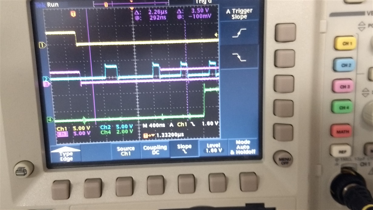
    The first 2 output bits returned should always be zero.

    The first is indeed zero but we sometimes see the second bit set.

    The attached shows SDO data is changing right on the clock falling edge.

    The datasheet timing diagram, (ADS7950 datasheet rev C, p. 18), shows SDO data should be set up and stable when the clock falls.

  • Were you able to move forward?

    I see that you clicked that this has been resolved

    SDO changes in the falling edge of SCLK and should be read in the rising edge of SCLK

    SDI also changes on the falling edge of SCLK and is read by the device on the rising edge of SCLK

    Regards

    Cynthia

  • Hi Cynthia--

    Yes I did get it working - solution follows if anyone else is interested.

    Thanks for your help!

    --Andy

    The problem: 

    The timing diagram in the datasheet indicates SDO data is set up and stable at the time the clock falls and for a while after.  Since this is driven by software things happen in sequence, so not possible to sample SDO at the same instant as the clock falling edge.  Previous code measured SDO after the falling clock edge, but the next data bit loads almost immediately so we got inconsistent results


    The fix: 

    We now delay a bit after raising the clock, test the SDO output, and then drop the clock back to low.


    #define ADC_DATA_IN_CH0_FWD_PWR2 0x1800   // bit 12-15 (0xF000) = 0001, Selects manual mode

    #define ADC_DATA_IN_CH1_FWD_PWR  0x1880   // bit 11 (0x0800) = 1, Enables programming of bits DI06-00.

    #define ADC_DATA_IN_CH2_REV_PWR  0x1900   // bit 7-10 (0x0780) = channel number 0-3, so only bottom 2 bits are used

    #define ADC_DATA_IN_CH3_ALC_OUT  0x1980   // bit 6 (0x0040) = 0, Selects 0 to VREF input range

                                              // bit 5 (0x0020) = 0, Device normal operation (no power down)

                                              // bit 4 (0x0010) = 0, Serial read of data from SDO

                                              // bit 0-3 (0x000F) = 0, Not used in our implementation


    static void getADC(ADC_CHAN chan)

    {

        int i=0;

        uint16_t dataIn = 0;

        uint16_t dataOut = 0;

        uint16_t top4bits = 0;

        uint16_t prevChan = 0;

        uint32_t iDelay = 0;   // Each iDelay++; is approx 20ns.


        switch(chan)

        {

        case ADC_CHAN0_FWDPWR2:

        case ADC_CHAN0_FWDPWR2_SAVE_RESULT:

            dataIn = ADC_DATA_IN_CH0_FWD_PWR2;

            break;


        case ADC_CHAN1_FWDPWR:

        case ADC_CHAN1_FWDPWR_SAVE_RESULT:

            dataIn = ADC_DATA_IN_CH1_FWD_PWR;

            break;


        case ADC_CHAN2_REVPWR:

        case ADC_CHAN2_REVPWR_SAVE_RESULT:

            dataIn = ADC_DATA_IN_CH2_REV_PWR;

            break;


        case ADC_CHAN3_ALC:

        case ADC_CHAN3_ALC_SAVE_RESULT:

            dataIn = ADC_DATA_IN_CH3_ALC_OUT;

            break;


        case ADC_RESET_REGISTERS:

            dataIn = 0x4200;

            break;


        case ADC_NOP_DELAY_FOR_CONSOLE_OUTPUT:

            return;


        default:

            debugAssert(false);

            break;

        }


        HAL_GPIO_WritePin(GPIOC, GPIO_PC10_OUT_ADC_SCLK, GPIO_PIN_RESET);  // ADC SCLK Low

        HAL_GPIO_WritePin(GPIOA, GPIO_PA15_OUT_ADC_CS, GPIO_PIN_RESET);    // ADC CS Low   


        dataOut = 0;

        for(i=0; i<16; i++)

        {      

            dataOut <<= 1;


            if(0 != (dataIn & 0x8000) )

            {

                // "MOSI" == "Master Output Slave Input" where "Input" is relative to the ADC device

                // In the GPIO pin name "..._OUT_..." is relative to the MCU

                // so GPIO_PD06_OUT_ADC_MOSI is data sent "OUT" from the MCU to the ADC MOSI input

                HAL_GPIO_WritePin(GPIOD, GPIO_PD06_OUT_ADC_MOSI, GPIO_PIN_SET);  // Send data bit to ADC (MOSI)

            }

            else

            {

                HAL_GPIO_WritePin(GPIOD, GPIO_PD06_OUT_ADC_MOSI, GPIO_PIN_RESET);

            }


            HAL_GPIO_WritePin(GPIOC, GPIO_PC10_OUT_ADC_SCLK, GPIO_PIN_SET);    // SCLK High   


            iDelay++;

            iDelay++;

            iDelay++;

            iDelay++;


            // Receive data bit from ADC (MISO)

            if(HAL_GPIO_ReadPin(GPIOC, GPIO_PC11_IN_ADC_MISO))

            {

                dataOut |= 0x1;

            }


            dataIn <<= 1;


            HAL_GPIO_WritePin(GPIOC, GPIO_PC10_OUT_ADC_SCLK, GPIO_PIN_RESET);  // SCLK Low                  

        }


        iDelay++;  // 26ns delay from 16th SCLK falling edge to 3-state

        iDelay++;


        HAL_GPIO_WritePin(GPIOA, GPIO_PA15_OUT_ADC_CS, GPIO_PIN_SET);  // ADC CS High   


        m_adcCmdSentCount[chan]++;


        top4bits = (0xF000 & dataOut) >> 12;


        switch(chan)

        {

        case ADC_CHAN0_FWDPWR2_SAVE_RESULT:

        case ADC_CHAN1_FWDPWR_SAVE_RESULT:

        case ADC_CHAN2_REVPWR_SAVE_RESULT:

        case ADC_CHAN3_ALC_SAVE_RESULT:

            prevChan = 0x3 & top4bits;   

            if(prevChan != top4bits)

            {

                m_adcIsValidValue[prevChan] = false;

                m_adcRcvFailCount[prevChan]++;

            }

            else

            {

                m_adcIsValidValue[prevChan] = true;

                m_adcValue[prevChan] = (0x0FFF & dataOut);

                m_adcRcvOKCount[prevChan]++;

            }

            break;


        default:

            break;

        }

        return;

    }