This thread has been locked.

If you have a related question, please click the "Ask a related question" button in the top right corner. The newly created question will be automatically linked to this question.

ADS5560: ADS5560 Problem

Part Number: ADS5560

Hi TI Team:

The customer has some problems when using ads5560, please help

Application scenario:

1. Differential input V + - v-input range [- 1.78-1.78];

2. Currently, the maximum input core signal frequency is 1MHz

3. External input single end 16mhz CLK, output use parallel CMOS,data acquisition adopts ADC CLK out

4. use internal reference 1.5V

5. Register configuration is as follows:

Output interface(Rigister6C D4-D3): 00 set cmos interface

Gain:(Rigister68 D3-D0):1000 set gain 0dB

LF.NOISE.SUPPRESSION:(Rigister5D D0):1 set Enable low-frequency noise suppression

Data format:(Register 63 D3):0 Set 2s-complement

REF:(Register 6D D4):0 Set internal refrence

LOW SPEED:(Register 63 D4):1 LOW SPEED mode eabled

STBY:(Register 63 D4):0 Normal operation

Current problems:

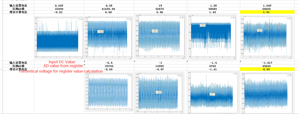
(1) Insufficient dynamic range

Root cause: fixed baseline, size 5400 AD

The analog input DC voltage is as follows, and the corresponding measured ad value is as follows


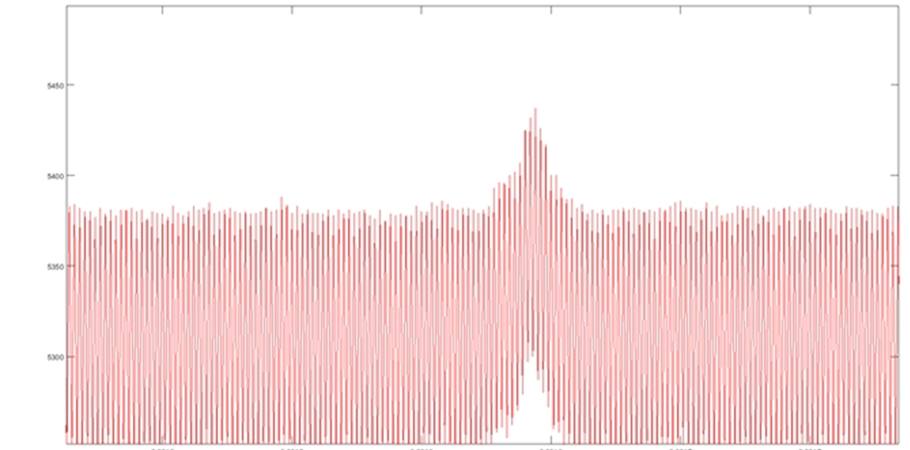
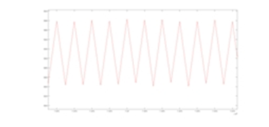
(2) The digital output signal has a fixed frequency of 8MHz noise (shown above after filtering)

after deployment, 8MHz frequency

(3) Question 3: ADC has low noise mode. What is the difference between on and off mode.

Thanks

CQ.LV

  • Hi CQ.LV,

    1) How is the ADC input driven? As a DC input signal is applied, I assume a differential amplifier used for driving input. When this data is collected, is the DC input voltage measured at the ADC pins or DC voltage at pins is calculated from voltage applied to amplifier input and amplifier gain? 

    The ADC full scale is 3.56 V p-p for 1dB and 0dB fine gain. This means that the output code range will be 58409 LSBs (or 1 dB below 65536) for 0dB fine gain. See section 7.3.2.4 of datasheet for details. 

    2) With sampling frequency of 16 MHz, the digital output FFT frequency band is from 0 to 8 MHz. So if there is a spur at the center of band as shown in the FFT, the spur is at 4 Mhz not 8MHz. This can be caused if a 4 Mhz clock frequency is used on board for some other device and noise at 4 MHz is coupling to ADC input.

    3) ADC has a low-frequency noise suppression mode. This is specifically useful in applications where good noise performance is desired in the low-frequency band of DC to 1 MHz.This mode is explained in section 7.3.1 in datasheet. In figures 43 and 44, blue plots are with LF noise suppression mode enabled and red plots are with LF noise suppression mode disabled