A related question is a question created from another question. When the related question is created, it will be automatically linked to the original question.
If you have a related question, please click the "Ask a related question" button in the top right corner. The newly created question will be automatically linked to this question.
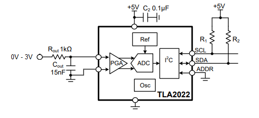
TLA2021: 0 - 3V signal input - HW and SW configuration
For a measurement of 0V to 3V, you would need to use the PGA, and therefore use the TLA2022. The TLA2021 only can be set to a full scale range of ±2.048V. For something larger in the TLA2022, you could use the ±4.096V range. Note that the ADC is fully differential and that it always measures AINP-AINN, so that 0V to 3V is represented as codes from 0000h to 05DCh so you have less than 11 bits of resolution. You can get the conversion information in the Data Format section in 8.5.3 of the datasheet.
The schematic that you might use looks something like this:
There an input RC filter, and bypass capacitance for the supplies. There are also pull-ups for the SCL and SDA lines for the I2C communication.
The TLA2022 uses a 16-bit configuration register. I would generally use the single-shot conversion mode. Here's a table of the register values for setting a data rate of 3300 SPS and an FSR of ±4.096V.
Bit
Field
Value
Description
15
OS
1
Start a single conversion
14:12
MUX[2:0]
000
Default input
11:9
PGA[2:0]
001
FSR = ±4.096 V
8
MODE
1
Single-shot conversion mode or power-down state (default)
7:5
DR[2:0]
111
DR = 3300 SPS
4:0
Reserved
00011
Always write 03h
Additionally, here is some basic pseudocode to show how you might repeatedly read from the device.
Configure microcontroller for I2C communication, I2C address=1001000 (48h) Loop { Send 90h 01h 43h E3h // // Start write to address 48h, write bit 0 (90h) // Configuration register 01h // Set 43E3h, AIN0-AIN1, FSR=±6.144V, Single-shot conversion, DR=3300SPS, stop Wait 353us // Wait for data period, +10% for internal oscillator variation, +20us Send 90h 00h 91h xxh xxh // Read back ADC conversion data // Start write to address 48h, write bit 0 (90h) // Conversion register 00h, stop // Start read from address 48h, read bit 1 (91h) // Read back 2 bytes, stop }
That should get you started. I took some of this from a cookbook circuit that you can find here:
The ADS1115 has a few extra features that aren't in the TLA2024, but they aren't used in the cookbook. Again, they can read through it and see if helps.
The schematic looks fine. With ADDR connected to GND, the address would be 1001 000. One thing that I wanted to know is what data rate they intend on using. Here the RC input filtering is set to 3.4kHz. Generally, I would set a bandwidth that is about 10x to 20x of the data rate. If they intend on using the 250SPS data rate this is fine. If they intend on using the 3300SPS data rate, I would reduce the input filtering capacitance to 47nF.