This thread has been locked.

If you have a related question, please click the "Ask a related question" button in the top right corner. The newly created question will be automatically linked to this question.

ADS1256: Lowest voltage the ADS1256 can measure

Part Number: ADS1256
Other Parts Discussed in Thread: ADS1255

Hi,

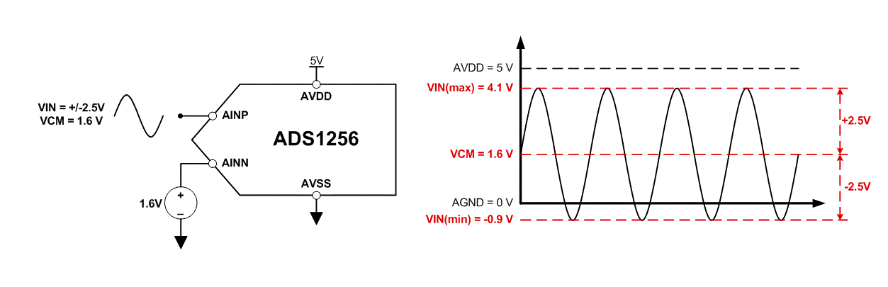
I have an ADS1256 that I want to use to measure microvolts amplitude signal ~5 uV pk-pk. According to the datasheet, with a data rate of 2000SPS and PGA = 1, the Input Referred Noise (μV, rms) with Buffer Off is 4.025 uV which according to a thread I've read is the  minimum voltage that the ADC can measure. I'm also a bit confused about the meaning of the full-scale range. When for example it says FULL-SCALE INPUT VOLTAGE VIN(1) (VREF = 2.5V) = ±78.125mV for PGA = 64 is this range from 0 to 156.25 mV or from 2.5V to 2.65625. Because my original small signal (~5uV pk-pk) was centered at 0 so I had to level shifted it so that it can be read by the ADS1256. The problem now is that the level-shifted signal isn't centered at 2.5 V or 78.125mV. The offset varies in terms of the input voltage. For a +/-2.5 V pk-pk signal, the level-shifted signal is centered at 1.6 V. 

  • Hi user,

    You are correct, the noise reported in the ADC datasheet (you are referring to Table 4) is the minimum ADC code resolution. If the ADC noise was 4 μVRMS and you applied a 0.4μV signal, the ADC could certainly read this input but wouldn't necessarily be able to distinguish it from a 0.8μV signal for example. Or, if you were trying to measure a 16μV signal and a 16.1μV signal, the ADC would not have enough resolution to determine that these signals were different, so they would both be grouped into the same code bin. You can reference our Precision Labs training for more information on this topic, specifically modules 4.2-4.4

    In your question, there are a couple of different concepts, including full-scale range (FSR), absolute input range, and common-mode range (VCM). For the ADS1256, these are:

    • FSR = ±2*VREF/PGA
    • Absolute input range = (AGND-0.1) to AVDD+0.1), assuming Buffer = OFF
    • VCM = same as absolute input range

    Note that this list is specific to the ADS1255 / ADS1256, and may not be the same for other ADCs.

    In your example, the full scale range given VREF = 2.5 and PGA = 64 is ±2*2.5 V / 64 = ±78.125mV as you noted. This sets limits on the VIN range you can apply to the ADC, where VIN = AINP - AINN. If AINP = 2.5V, then AINN must be somewhere in the range of 2.5V - 0.078125V and 2.5V + 0.078125V. If your VREF voltage and PGA gain were different, the FSR would be different as well. But the FSR is always determined by this equation.

    If you are using AVDD = 5V with buffer = OFF, the absolute value of your input signals must be > -0.1V and <5.1V. That means you could apply 0V to AINP and 1V to AINN such that VIN = -1V. But you could not apply -1V to AINP (or AINN) and 0V to AINN, since the ADS1256 cannot accept voltages below AGND

    Now, since VCM is the same as the absolute input range on the ADS1256, that means your signal VCM can be anywhere in this range as long as the other conditions are met (FSR, AIN range, etc). Taking your question about ±78.125mV - it is possible to have inputs as extreme as AINP = 0V and AINN = -0.078125V all the way up to AINP = 5V and AINN = 5.078125 V, since there is some small headroom beyond the supplies with buffer = OFF. However, any variation in supply/input/VREF voltage might shift these values outside of the ADC's datasheet specs, and is not recommended. This is simply to show what is possible given the wide VCM range on the ADS1256. If you had a ±2.5V signal centered at = 1.6V, this yields absolute input voltages of 4.1V (max) and -0.9V (min). This is not allowable as you can now see.

    I would recommend checking out the ADS1256 calculator so you can play around with the input settings to make sure they do not violate the ADC's requirements.

    -Bryan

  • Hi Brian,

    Thanks for clarifying my confusion between input noise and minimum ADC resolution. I now have a better understanding on how to properly set up the device to read various voltage ranges. I'm still a bit confused about AIN range, you mentioned that with the ADS1256, we can read voltages as low as 0 V on AINP and -0.078125 V on AINN. Is this only achievable using differential mode or can I still do it using the single-ended mode? 

    If I have a 80 uV pk-pk signal centered at 40uV does that mean if I usea date rate of 10SPS and a PGA Gain of 8  (with buffer OFF) I can clearly see the signal as opposed to using date rate of 10 SPS and PGA Gain of 1 (with buffer OFF). Also, will I get the same result if the signal  was centered at 2.5V instead?

    I don't quite understand how calculated the absolute input voltages of -0.9V(min) for a +/-2.5 V signal centered at 1.6V. Shouldn't it be 2.5-1.6 = 0.9 V(min)?

    Thanks

  • Hi User,

    The ADS1256 always performs a differential measurement, in that the ADC is always sampling the difference between AINP and AINN, regardless of the input channels you have selected. If the analog input connected to AINN is at 0V, then this is a single-ended measurement, but the ADC is always sampling in a differential manner. But a single-ended measurement will only provide half of the available code range, since the available code range extends from +2*VREF/PGA to -2*VREF/PGA. You could only use a maximum of 0 V to +2*VREF/PGA in this case.

    The first image below is how I would expect your ADC connections and signals to look like given the +/-2.5V signal centered at 1.6V. If I made any incorrect assumptions, please let me know. Your VCM signal is with respect to AGND, so this is 1.6V above AGND as shown in the plot on the right. As the signal swings to -2.5V, you would apply -0.9V to the ADC input, which is not allowed.

    Your 80μVPP signal centered at 40μV means your absolute input range will swing from 0 V to 80μV, assuming you did not mean +/-80μVPP. So you are at the very bottom of the allowable input range, but it still works. As stated previously, the ADS1256 VCM range is very wide, so you have a lot of flexibility here. But for many ADCs you would try to ensure your signal VCM is close to the ADC VCM, which is generally (AVDD-AVSS)/2.

    The second image below represents a digitized sinewave. The ADC noise (resolution) represents the width (not height) of each "stair". So it effectively determines into how many pieces (codes) you can break the input signal. As you can imagine, a lower resolution ADC would have much wider "stairs", and the resulting digitized signal would not look much like a sinewave at all. Again, please refer to the Precision Labs modules for more info on this topic.

    Hopefully these visualizations help make this more clear.

    -Bryan