This thread has been locked.

If you have a related question, please click the "Ask a related question" button in the top right corner. The newly created question will be automatically linked to this question.

ADS1278: Reading data in SPI fixed mode

Part Number: ADS1278
Other Parts Discussed in Thread: ADCPRO, SN74HC595

Hi,

i want to get data from ADS1278 EVM in SPI mode.

I have used EVM-PDK as power supply and raspberry pi as data extractor, as the picture shows:

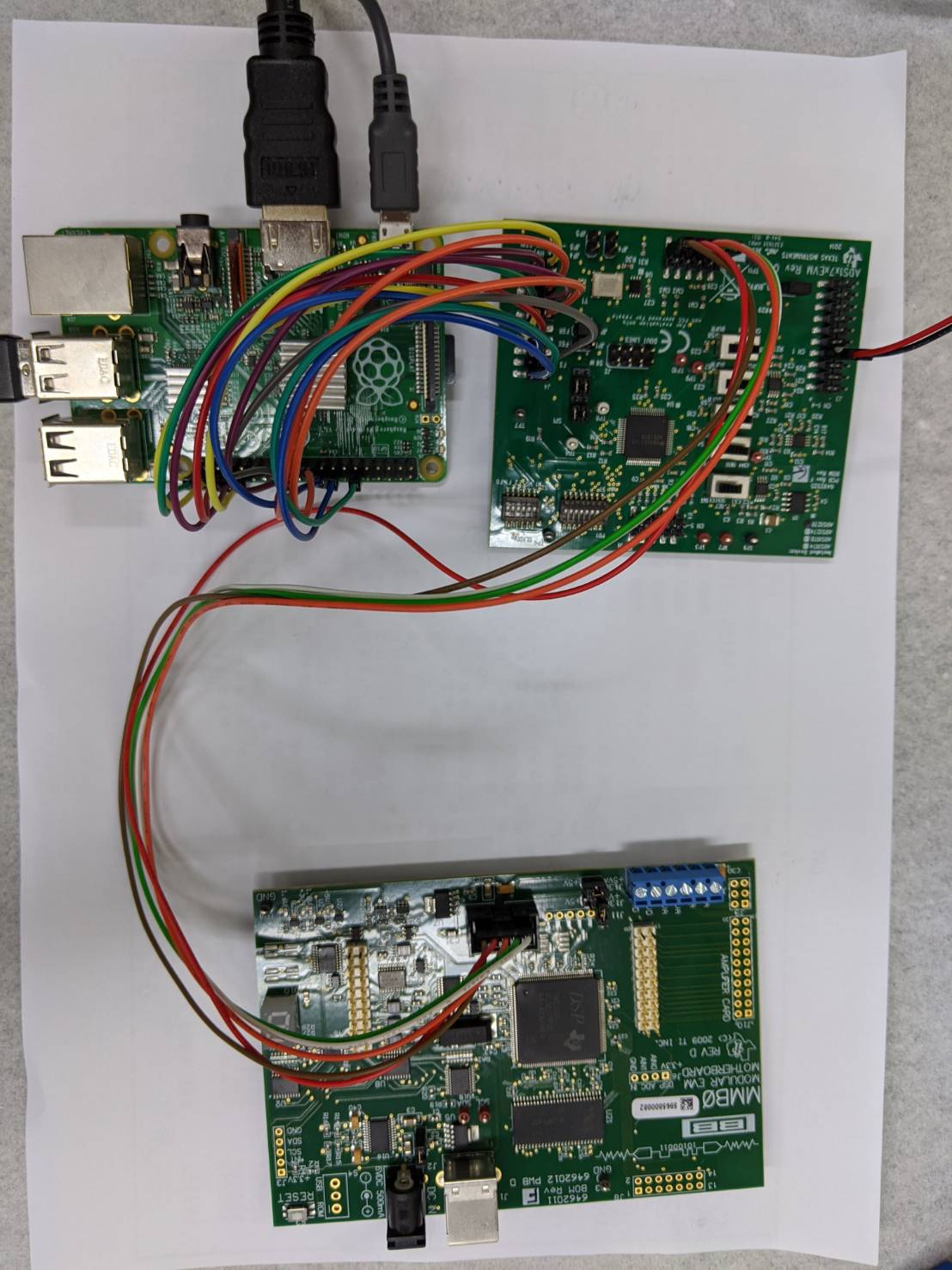
I'm sure the hardwares are normal, but i can't capture data from ADS1278EVM.

I think I have errors in wiring or software.

I would like to ask you to provide some comments about it.

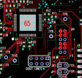
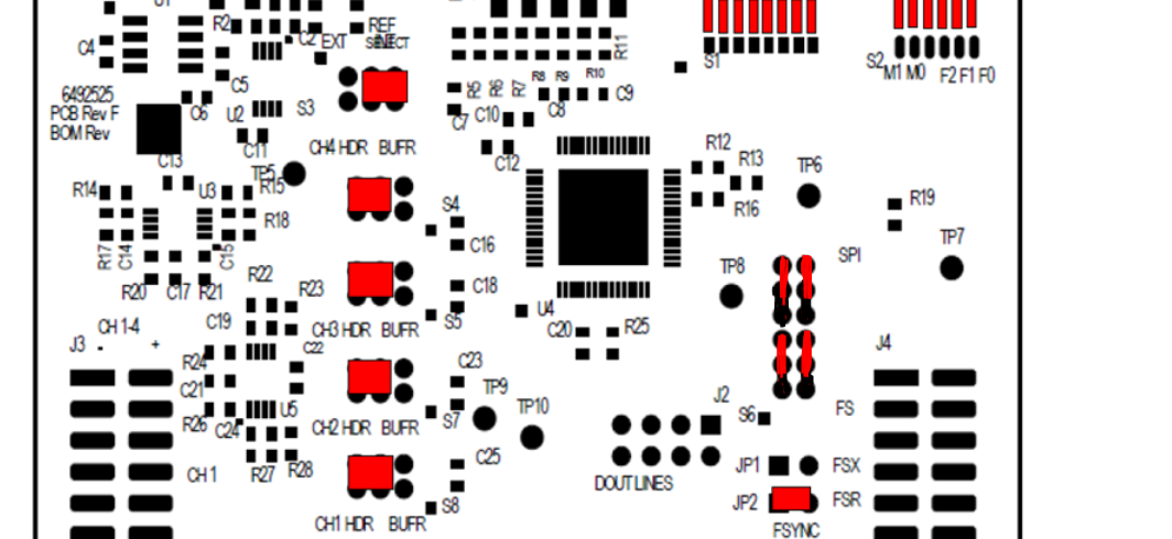
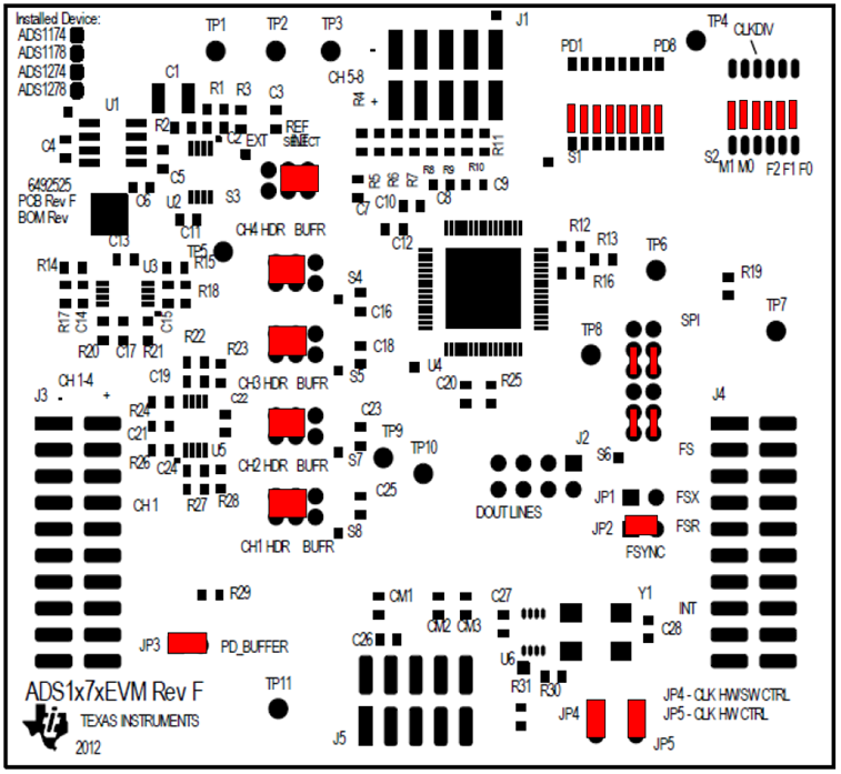
Here are all my wiring and settings:

S6 -> turn to SPI

JP4, JP5 -> open circuit

J3.7, J3.8 -> connect photodiode (1channel)

J4.2, J4.6 -> [0,1] High-Resolution

J4.8, J4.12, J4.14 -> [0,0,1] SPI TDM Fixed

J4.1 -> High (SYNC)

J4.19 -> High (CLK)

J4.15 -> start to capture data when voltage falling (DRDY)

J4.3 -> SCLK pin on Rapberry Pi

J4.13 -> MOSI pin on Rapberry Pi

J4.18 -> GND pin on Rapberry Pi

J5.3, J5.5, J5.7, J5.9 -> connect EVM-PDK

But it doesn't work with this setting.

I don't know where is the problem ?

Can you please help me to solve it ? Thank you.

  • Hello,

    Can you take some measurements and verify the signals are getting to the IO pins of the aDS1278?  An oscilloscope or a logic analyzer could be used to verify communications.

    Also, from your above list:

    J4.13 -> MOSI pin on Rapberry Pi

    This is incorrect, and should be connected as shown:

    J4.13 -> MISO pin on Rapberry Pi

    Regards,
    Keith Nicholas
    Precision ADC Applications

  • Hi,

    I use multimeter to ensure that these I/O pins are triggered by  raspberry pi.

    But I still did not capture any signal from the DOUT pin.

    In this state, DOUT pin has no voltage value,

    but it has the voltage value when connected to EVM-PDK.

    I guess i have something unset but i don't know.

    Maybe S1 or S2 should be changed or not ?

    Can you please help me to solve it ? Thank you.

  • Hello,

    Make sure your FORMAT pins are set to the correct levels for SPI TDM Fixed:

    FORMAT2 (J4.14)->0

    FORMAT1 (J4.12)->0

    FORMAT0 (J4.8)->1

    Also, MODE pins are set correct levels for High Resolution:

    MODE1 (J4.6)->0

    MODE0 (J4.2)->1

    S1 and S2 should all be set to the OFF condition.

    S6 should be set for SPI mode:

    jumpers installed on [2-3], [5-6], [8-9], [11-12]

    Regards,
    Keith

  • Hi, Keith:

    Thank you so much for helping out !

    I successfully capture data from ADC.

    Another small question, how can i control the power on or down of CH1~8 just like ADCPro ?

    And can i reset ADC by trigger pins on ADS1278 EVM ?

    Thanks again !

  • Hello,

    The ADS1278EVM uses an IO expander device over I2C.  The only way to control power up/down for the ADS1278 is through 8 GPIO lines.  You can either directly provide these IO signals from your MCU, or use something similar to the EVM.  Since you are already using SPI, you could just use a serial shift register, such as SN74HC595.

    The ADS1278 has a /SYNC pin that can be used to reset the internal digital filters and start a new conversion.

    Regards,
    Keith 

  • Hi, Kieth :

    Thank you for your reply.

    If i don't make any settings, does it mean that 8 channels are continuously power up ?

    So that can i restart the ADC by raising the voltage of the SYNC pin ?

    Another question about data format from ADS1278s, i can capture data by SPI TDM Fixed mode now.

    I capture 3 bytes data as a piece of data, then i combined this data into a 24-bits in binary and performed 2's complement operation.

    Therefore, i receive 24 bytes data (192 bits) as a round of 8 channels of data.

    For example, i capture 3 bytes data : [250,250,10]

    250 => 11111010 ; 10 => 00001010

    So i combined this data into [11111010 11111010 00001010] and got the value [-329206] based on the two's complement.

    Further calculated the voltage is -329206 * 2.5 / (2^23-1)= -0.098 .

    But sometimes i get unreasonable values.

    Are there problems with the way i capture or calculate the data ?

    Thanks for your help !

  • Hello,

    There are no configuration registers in the ADS1278.  The channels are ON if the /PWDNx pins are pulled high, and they are OFF if the corresponding channel pin is pulled LOW.  If you always want the channels ON, you can simply tie each of the /PWDN pins to IOVDD.

    Your calculations are correct.  It is possible you are getting bit errors when reading the values.  This can easily occur based on the picture of your setup using high speed clocks.  As a test, you could slow down the MCLK and SCLK to 1MHz, and see if the readings are more consistent.

    Regards,
    Keith

  • Hi, Keith :

    Thanks for your solution and suggestion.

    But i still couldn't get the correct data after I changed the setting for SCLK.

    My settings and python code are provided below.

    (red words represent comments)

    ################################################################################

    #!/usr/bin/env python

    import RPi.GPIO as GPIO
    import spidev

    # SPI setting
    spi = spidev.SpiDev()
    spi.open(0,0)
    spi.max_speed_hz = 7800000 #SCLK frequency
    spi.mode = 0b00 #C_POL=0, C_PHA=0
    spi.no_cs = True

    # get bytes
    def adc_1ch(): #1channel
        data = spi.xfer([0x00,0x00,0x00]) #24bits = 3bytes
        adc = (data[0] << 16) + (data[1] << 8) + data[2] #shift register
        if adc > (2**23-1): #2's complement
            adc = adc - 2**24
        voltage = (adc*2.5)/(2**23 - 1)
        return voltage

    def adc_8ch(): #8channel
        ch = []
        for i in range(8):
            ch.append(adc_1ch())
        return ch

    # GPIO setting
    GPIO.setmode(GPIO.BOARD)
    pins = [12,16,18,36,38,40,32] #SYNC, MODE*2, FORMAT*3, CLK Select pin
    volt = [1,1,0,1,0,0,1] #1=high, 0=low
    for p in range(7):
        GPIO.setup(pins[p],GPIO.OUT)
        if volt[p]==1:
            GPIO.output(pins[p],GPIO.HIGH)
        else:
            GPIO.output(pins[p],GPIO.LOW)

    GPIO.setup(22,GPIO.IN) #DRDY pin

    # main
    i = 0 #timer
    while True: #loop 100 times
        GPIO.wait_for_edge(22, GPIO.FALLING) #start to capture data when DRDY falling down
        print(adc_8ch()) #capture data
        i = i + 1
        if i == 100: #timer stop
            break

    GPIO.cleanup()

    ################################################################################

    Are there any errors in my settings or logic ?

    Thank you so much again.

  • Hello,

    Your code looks correct, but I cannot exactly follow it.

    Use a DMM and check all of the configuration pins to confirm you have the correct logic values.  (SYNC, MODE, FORMAT, CLKDIV).

    If possible, find a logic analyzer or oscilloscope and capture /DRDY, SCLK, DOUT so we can verify all timing requirements are met.

    Regards,
    Keith

  • Hi, Keith :

    Thanks for your help.

    I don't know how to set CIKDIV on ADS1278EVM.

    Could you help me to set CIKDIV ?

    Nonetheless, I used DMM to detect that the CIKDIV on ADS1278s chip has voltage.

    And i saw the following statement from the document :

    In the SPI format, DRDY goes high as soon as SYNC is taken low; see Figure 73. After SYNC is returned high, DRDY stays high while the digital filter is settling. Once valid data are ready for retrieval, DRDY goes low.

    Is that mean i shouldn't keep setting pin SYNC voltage high ?

    And is there any specific command to be passed to the ADC to get the correct value?

    I just send 24 times 0x00 to ADC now.

    I'm sorry I don't have a logic analyzer or oscilloscope to capture the signal graph...

    Thank you again.

  • Hello,

    There are no commands to send to the ADS1278.  All modes of operation are configured by connecting pins on the ADS1278 to GND (0V) LOGIC 0 or IOVDD(I assume you are using 3.3V for IOVDD) LOGIC 1.

    You can set CLKDIV on the ADS1278EVM using S2.

    S2-4 OFF, CLKDIV LOW

    S2-4 ON, CLKDIV HIGH

    You state that CLKDIV has voltage, so I assume it is HIGH, which means you will get the following data rates.

    High-Speed Mode:  fDATA=fCLK/256

    High-Resolution Mode:  fDATA=fCLK/512

    Low-Power Mode:  fDATA=fCLK/512

    Low-Speed Mode:  fDATA=fCLK/2560

    The ADS1278 will continuously convert data as long as SYNC is held high.  If you keep SYNC high all of the time, your MCU should monitor /DRDY, and when it goes LOW, you can then send 24*8=192 SCLK's to clock out the data from all 8 channels.

    DIN should be connected to GND unless you are trying to daisy-chain more than 1 ADS1278 to the same SPI bus.  DIN is only used to daisy-chain multiple ADS1278 devices, there are no internal registers or commands to write to the ADS1278.

    Regards,
    Keith

  • Hi, Keith :

    Thanks for your reply.

    Is that mean i can set S1 and S2 to control ADS1278 EVM ?

    So that i can change my settings like this :

    S1 -> turn on all

    S2 -> M0,CLKDIV,F0 turn on, others still turn off

    S6 -> turn to SPI

    JP4, JP5 -> open circuit

    J3.7, J3.8 -> connect photodiode (1channel)

    J4.2, J4.6 -> [0,1] High-Resolution

    J4.8, J4.12, J4.14 -> [0,0,1] SPI TDM Fixed

    J4.1 -> High (SYNC)

    J4.19 -> High (CLK)

    J4.15 -> start to capture data when voltage falling (DRDY)

    J4.3 -> SCLK pin on Rapberry Pi

    J4.13 -> MISO pin on Rapberry Pi

    J4.18 -> GND pin on Rapberry Pi

    J5.3, J5.5, J5.7, J5.9 -> connect EVM-PDK

    =================================================================

    But there is a caution in document for ADS1x7xEVM-PDK.

    So i'm not sure if my new settings will cause component damage?

    Thanks for your help again.

  • Hello,

    Yes, you can use S1 AND S2 to configure the device when not using the MMB0 board.

    S1 -> turn on all


    NO, In order to turn all channels ON, all S1 switches must be set to OFF.  (These are negative logic.)

    S2 -> M0,CLKDIV,F0 turn on, others still turn off


    YES, these switches will configure the mode and format settings.  For the above switch settings:

    MODE=01 (High Resolution), CLKDIV=1, Output Data rate fDATA=52734sps when fCLK=27MHz.

    FORMAT=001, SPI mode, TDM (all data output on DOUT1), Fixed position

    S6 -> turn to SPI


    Yes, set S6 jumpers to SPI mode per below:

    All other settings look correct to convert readings on Channel 0.

    The caution statement only applies when the ADS1278EVM is plugged into the MMB0 board.  Since you are only using the MMB0 for the power connections, you can set the switches S1 and S2 as needed.

    Also, you stated that you are using a photodiode.  The inputs of the ADS1278EVM need a low impedance source voltage.  The output of a photodiode is a high impedance current source.  You will need an additional amplifier circuit for the photodiode, before connection to the ADS1278EVM.

    Please refer to the following cookbook circuit for an example.

    https://www.ti.com/lit/an/sboa220a/sboa220a.pdf

    Regards,
    Keith

  • Hi, Keith :

    I tried to turn off only channel 5 by setting S1 switch,

    and i still used SPI TDM fixed mode and high resolution mode.

    However, i got sometimes the error data like this :

    I guess the data I read is shifted, but the shift is random.

    Do you have any experience or methods to solve this situation ?

    Thanks for your reply again.

  • Hello,

    If you do not read all data out of the ADS1278 before the next data conversion results are ready (the next DRDY low), then you could get corrupted data.  It is hard to guess without seeing the timing waveforms for DRDY, CLK, DOUT.

    You can slow the conversion rate down by using a much slower CLK frequency, but this will require an external clock generator, or changing the oscillator on the ADS1278EVM board to a different value.

    Regards,
    Keith

  • Hi, Keith :

    If i want to replace the 27MHz oscillator on-board with an external clock,

    i guess i must change some settings on ADS1278EVM.

    But i'm not sure if my configuration is correct, the following:

    JP4 => Open

    JP5 => Short

    J4,17 => Connect external oscillator

    J4,18 => Connect ground from external oscillator

    J4,19 => don't connect anything

    Is that right ?

    Thanks for your help very much.

  • Hello,

    Yes, you are correct.

    However, the inputs for U13 should not be floating.

    Please connect J4,19=>Ground

    Regards,
    Keith