


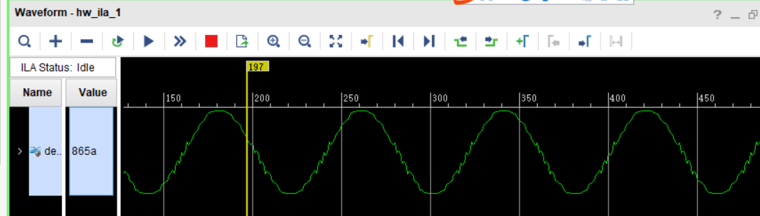
At present, Xilinx's FPGA is used in the ads5560 acquisition scheme, and there is a problem of the distortion of the collected sine wave data.
When the ads5560 is configured as a test mode, the data and the data mode mentioned in the specification are completely corresponding to the error free mode.
In all 0s test mode, the 16 bit AD data received by FPGA is always 0
In all 1s test mode, the 16 bit AD data received by FPGA is always 1
In toggle pattern test mode, the 16 bit data received by FPGA will be 0x5555 to 0xaaaa alternately.
In the ramp Peter test mode, the 16 bit data received by fgap is from 0x0000 to + 1 to 0xFFFF.
All of the above four test modes are 0-bit error, so it is considered that there is no problem in the signal quality and internal acquisition timing of a pile of 1 LVDS clock and 8 LVDS data signals transmitted by FPGA through ad.
Under the condition that it has been determined that the digital transmission error between ads5560 and FPGA is zero, what factors may cause the waveform distortion of ads5560 in the working mode? In terms of the collected data, it is not like the bottom noise of analog circuit. Is it the chip configuration problem of ads5560 or the hardware design problem of analog circuit that causes the analog-to-digital conversion of ads5560 to be the data output by itself Is there a problem?
After all, the current test can think what value is on the digital pin of ads5560 and what value is definitely collected by FPGA. Because all four digital test modes can pass without error.
The waveform of analog port can be measured by oscilloscope. The continuity of analog circuit, even if the circuit has bottom noise, should not cause the data fault type abrupt change of ad digital terminal.
