This thread has been locked.

If you have a related question, please click the "Ask a related question" button in the top right corner. The newly created question will be automatically linked to this question.

ADS1263: DOUT/DRDY line does not follow the dedicated DRDY line when CS is active (low)

Part Number: ADS1263

Hello,

Running ADS1263 and getting everything working good in waiting/polling mode.

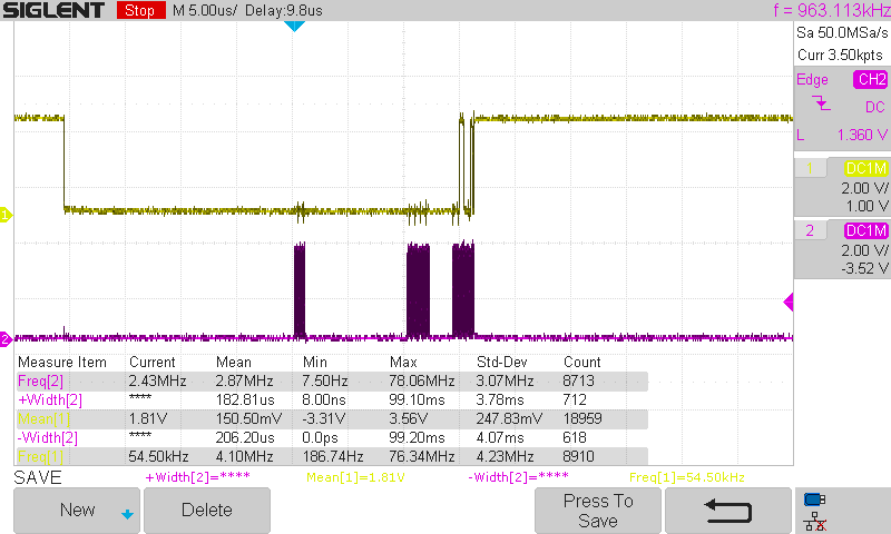
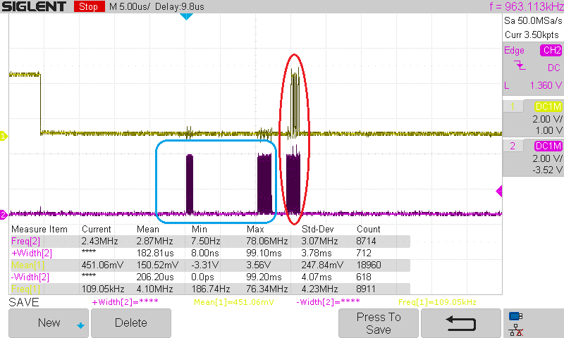
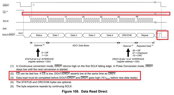
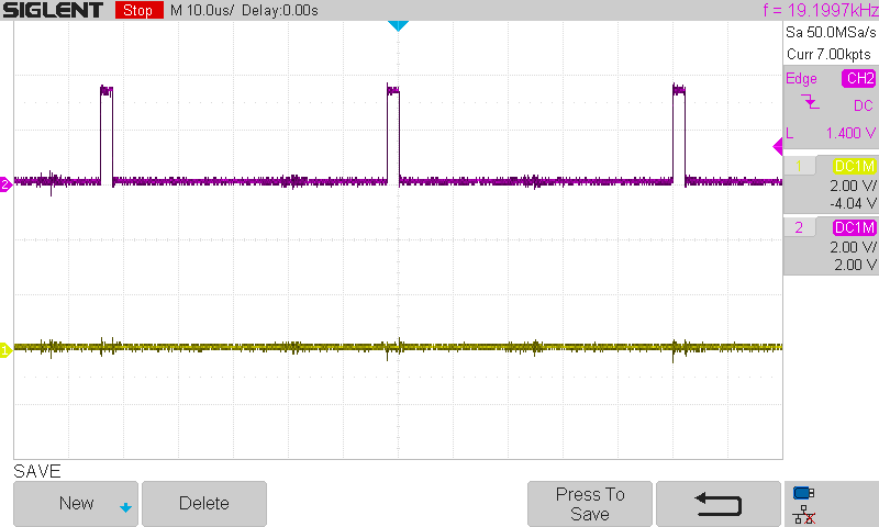
When using interrupts on DOUT/DRDY line however the line seem to keep the last data bit instead of following the dedicated DRDY line. So, setting an interrupt on the DOUT/DRDY line and getting CS low half times (when last bit was low) it fires immediately instead of waiting for the new data ready.

The dedicated DRDY line works perfectly fine, however by design I was supposed to rely on the DOUT/DRDY and MCU does not have access to dedicated DRDY line.

Am I missing something?...

Thank you for your help,

A.

  • Hi Anatoly,

    Can you please provide timing plots including /DOUT/DRDY, SCLK and /CS? Also, can you please clarify " CS low half times (when last bit was low)"?

    Thanks&regards,

    Dale

  • Hi Dale,

    Thank you for helping with this. I also submitted a formal ticket on TI support…

    While dedicated DRDY pin works exactly as described, DOUT/DRDY pin works as described only if the last shifted bit from that pin during SPI transaction was “1” or high.

    If the last shifted bit from DOUT/DRDY was 0, the DOUT/DRDY pin stays at “0” even when digitizing is not finished and when dedicated DRDY pin is high (this is in case I keep /CS low all the time).

    If the last shifted bit from DOUT/DRDY was 0, when setting /CS high for a period of time after reading the data the DOUT/DRDY pin goes to “0” immediately after turning /CS low again even if the digitizing is not finished and dedicated DRDY pin is still high. That is causing a premature interrupt when /CS goes low.

    Thank you very much for your time and help,

    Anatoly


    DOUT/DRDY (yellow, ch1) and SCLK (purple, ch2) when last shifted bit is “1”


    DOUT/DRDY (yellow, ch1) and SCLK (purple, ch2) when last shifted bit is “0”


    /CS (yellow, ch1) and SCLK (purple, ch2)

  • Hi Anatoly,

    Thanks for your information. Did you start a new conversion by the START pin or by serial commands before you turn /CS low again?

    You are reading the data highlighted in red, what's the operation for the SCLKs highlighted in blue? Are you using a voltage level to trigger an interrupt? a timing plot captured for the following frame is helpful. 

    Best regards,

    Dale

  • Hi Dale,

    Thank you for the reply.

    My START pin is tied to GND (via 50-ohm resistor), and I am using the command to start conversion. Also, most of the time the ADC is in the free running mode, so I just read out data using READ ADC1 command. However, also tried doing a direct buffer read without command, the results are identical – when last bit is “0” the DOUT/DRDY line is not working as expected.

    Dale, your question about red/blue highlighted data is not clear for me. I am using a low-going (“1” to “0” transition) interrupt on my MCU on the DOUT/DRDY line. If you could re-phrase the last question, I can capture necessary diagrams.

    One more comment. I found a temporary way to work with the situation. After reading the data from the buffer, to read a register that has “1” as an LSB. Specifically, I am reading IDACMUX register with default value of 0xBB or the last bit of “1”. After adding this dummy read interrupt works as desired every time. I know this is just a temporary solution until you could confirm that it can be used reliably.

    Thank you,

    Anatoly


  • Hi Anatoly,

    Apologized for missing the graph, please see my question with the graph below.

    Best regards,

    Dale

  • Hi Dale,

    Thank you for clarifying.

    The blue data is OPCODE 0x12 and shift of the first two data bytes and the red are the last two bytes of the data. The transfer looks perfectly fine and for the transaction on the picture the STATUS and the CRC are disabled, so the entire transaction is 5 bytes.

    The actual received data seems to be of high quality as expected.

    The only situation I have since the last shifted bit is more or less always noise it is a random “0” or “1”, so when it is “0” then I cannot use data ready interrupt on this line.

    Could you confirm you have similar behavior or such behavior is not typical?

    Thank you,

    Anatoly

  • Hi Anatoly,

    I'm checking with my colleague who has more experience on this ADC, I will get it back to you soon, thanks for your patience.

    Best regards,

    Dale

  • Thank you, Dale, really appreciate your help.

    Let me know if I could help with any additional tests...

  • Hi Anatoly,

    Is your ADC working in Continuous Conversion Mode or  Pulse Conversion mode (RUN Mode in Mode 0 register)? Did you send a START1 command for a new conversion before you send another READ ADC1 command to read the data during next cycle? The next cycle I'm talking is the cycle after the DATA READ cycle your are showing in your timing, which is also the cycle you are detecting the falling edge (“1” to “0” transition) on the DOU/DRDY pin.

    Regarding the timing in Figure 108 and 109, the /CS needs to stay low. If the /CS is held low, DOUT/DRDY will eventually return high before the next conversion result is ready. Therefore, it may hold the value of the LSB, however it should return to high before the next conversion result is ready, see the footnote 3 below:

    Also, you are using the falling edge to trigger the interrupt in your controller, there is another way to detect and read the data on DOUT/DRDY pin, you can monitor this pin in either Read Data by Command or Data Read Direct mode, the DOUT/DRDY is driven low if the /CS is held low.

    Best regards,

    Dale

  • Hi Dale,

    I think you got it.

    If the last shifted bit was “0”, DOUT/DRDY would return high only 16 cycles before data is ready. So, I have to keep /CS low to be able to use the going low interrupt when the next data is ready.

    It will take me a few days to re-configure and test everything, but I believe it will work.

    Thank you very much for looking into this and for your help with my question.

    I will confirm and close this case as resolved in a few days if everything works.

    Thank you,

    Anatoly

  • Hi Anatoly,

    Thanks for your experiment. Please let me know when you have a result, thanks.

    Best regards,

    Dale

  • Hi Anatoly,

    I had more discussions with team members, the pulse returning back to high on the DOU/DRDY signal is narrow, the GPIOs without specific capturing functionality on many controllers usually can not capture is properly, thus reading a particular internal register (e.g. IDACMUX) that has a "1" as an LSB is the only and good way to force the DOU/DRDY signal back to high. Thanks for your patience.

    Best regards,

    Dale

  • Hi Dale,

    Thank you very much for looking further into it!

    Yes, did quite a few experiments and with 200MHz scope could not see or trigger to the returning pulse on DOUT/DRDY line while I see a very clear pulse on the dedicated /DRDY line (without reading out the data it is 2us wide or ~16 cycles).

    Tried a bunch of several rates and different settings…

    So, you are correct, the MCU does not see the pulse or gets an interrupt after last shifted bit was “0”…

    However, the way you described of reading IDACMUX register after the data was read seems to work every time. So, if you could confirm with the designers that this is a reliable way to work with this ADC then we do have a good solution. Just want to make sure I don’t have a hidden or time delayed problem with my design/realization.

    Attaching a scope shot at 19.2ksps with ch1 (yellow) DOUT/DRDY line and ch2 (pink) is dedicated /DRDY line…

    Again, thank you very much for all your help and time with this situation!

    Anatoly


  • Hi Anatoly,

    I have confirmed that reading a particular internal register that has a "1" as an LSB is the only and good way to force the DOU/DRDY signal back to high. You can select and use a register which is not used for your normal configuration. Thanks.

    Best regards,

    Dale

  • Hi Dale,

    Perfect, thank you for confirming. This resolved my situation.

    Thank you for all your help with my question,

    Anatoly