


Other Parts Discussed in Thread: ADS1299
Tool/software: Code Composer Studio
I want to read the external signal through CCS. I have successfully read the internal test square wave as shown in figure 1 below, but when I changed the register to read the external signal 100 HZ SIN wave, the data output figure is as shown in figure 2. What is the reason? How can I improve this result?
Figure 3 shows the results of the external test signal presented on the oscilloscope.
figure 1
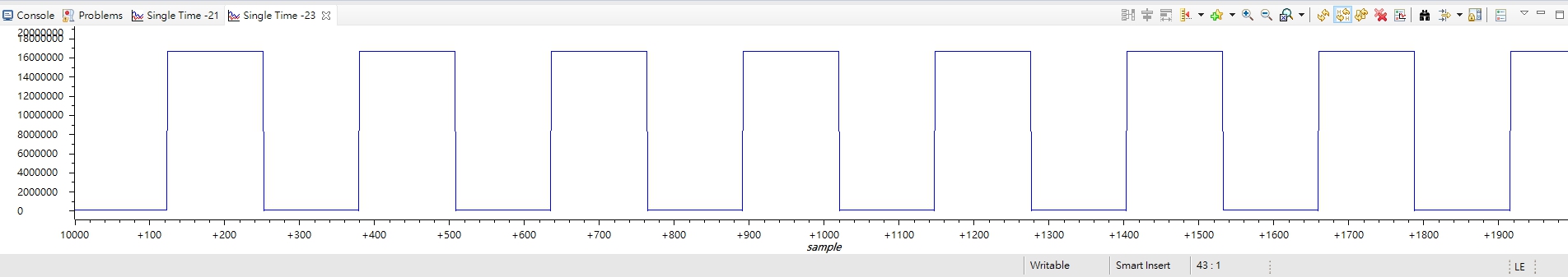
figure 2

figure 3


