This thread has been locked.

If you have a related question, please click the "Ask a related question" button in the top right corner. The newly created question will be automatically linked to this question.

ADS122U04: ADS122U04 Communication and Device Setup

Part Number: ADS122U04

Hello Bob,

Extremely thankful to you for replying to my query in a easy-to-understand way-
and almost zero turn-around time.
Now I am clear about how to derive the temperature value from the A/D code.
Now, first, I will reply to questions asked by you above and then ask one another query (Confusion about IDAC).
To answer your questions:- 

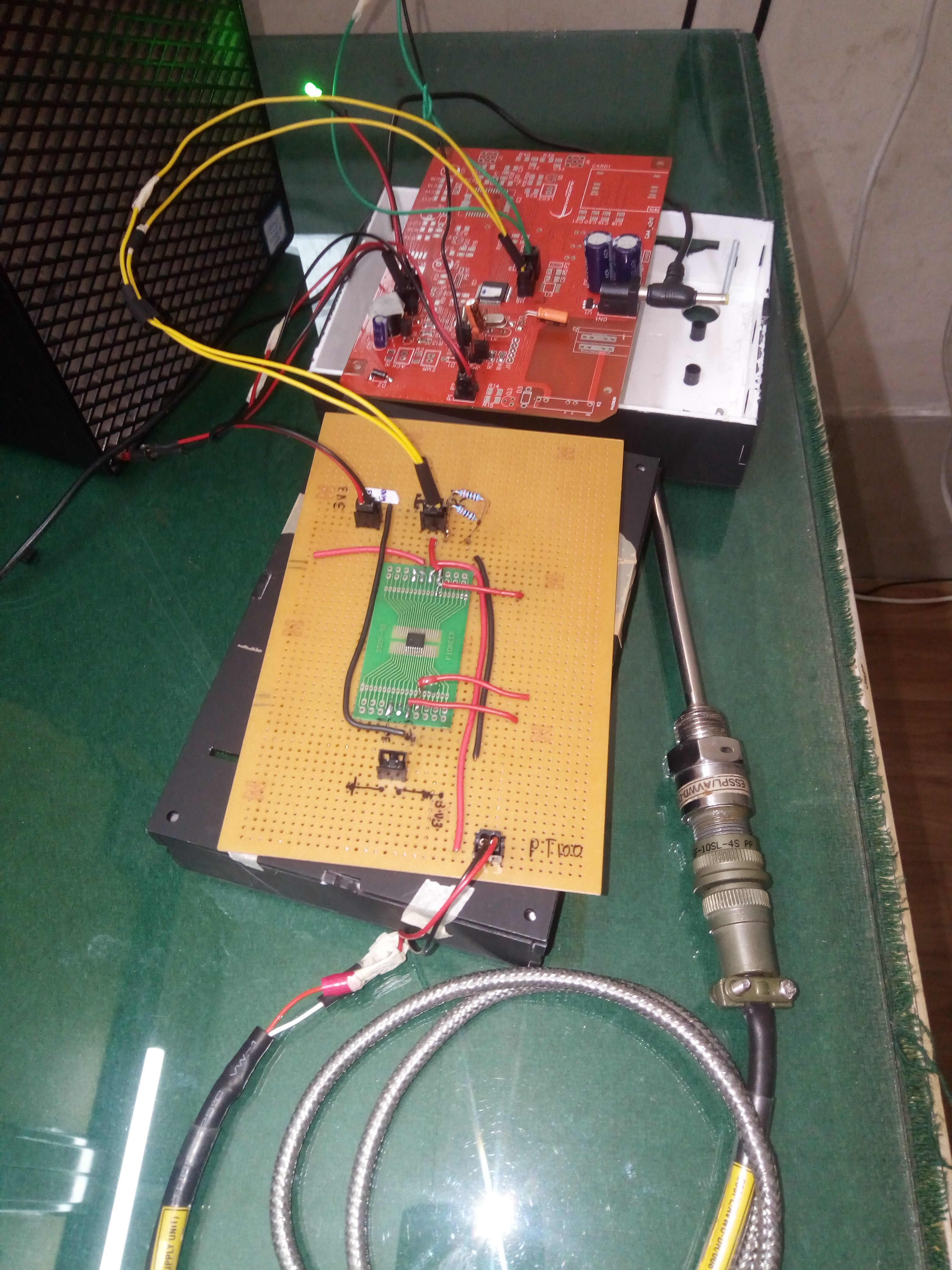
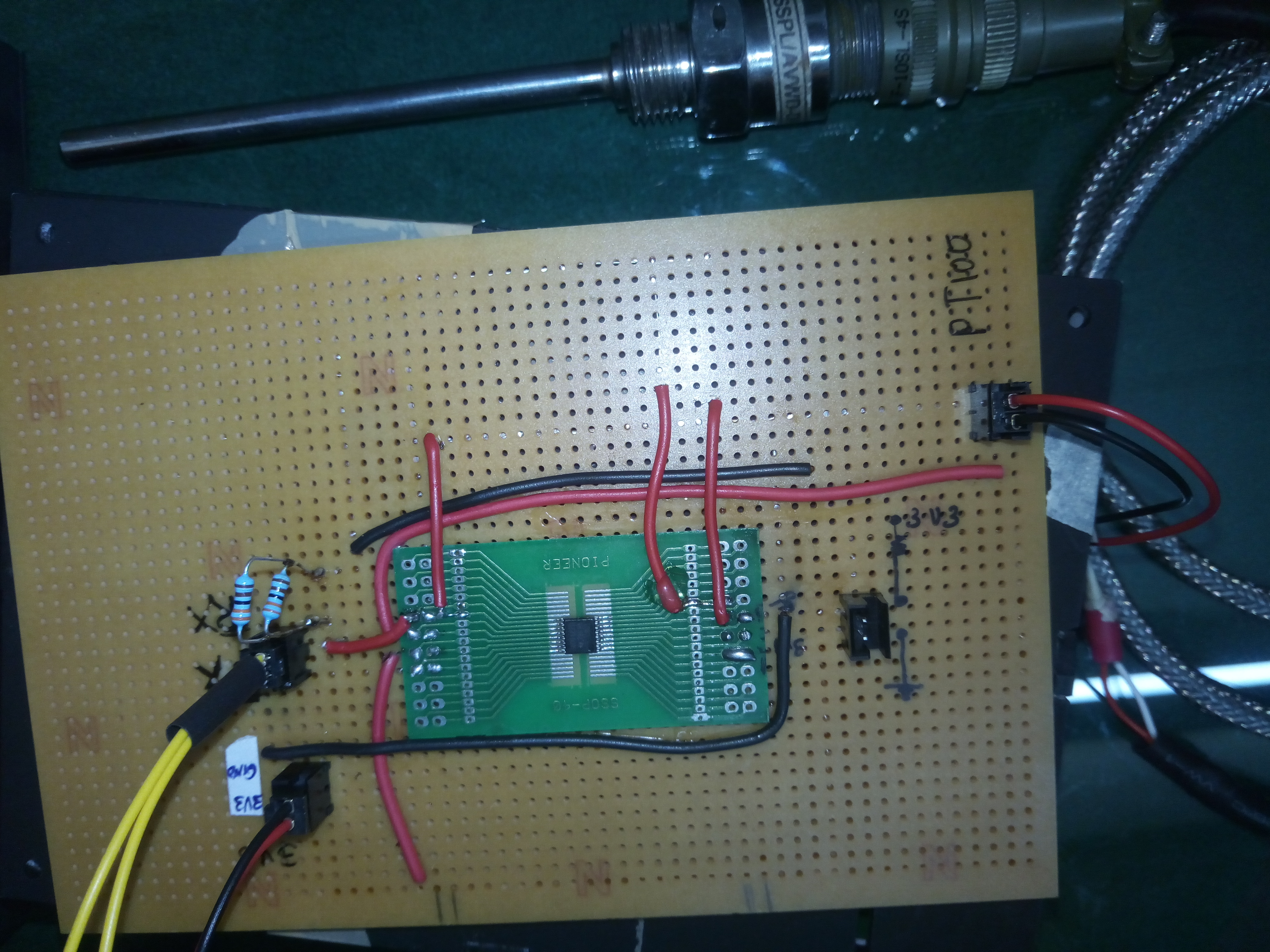
Yes, I am using 2-Wire RTD configuration with a single IDAC.
I have not populated the filter circuits (across RTD and Rref) yet, as I am still working on the core part.
Yes, I also am doubtful whether the return value of D4CA62 is a negative value, but the ambient temp.
at my desk is (30 DegC) [Indian Monsoon season and AC turned OFF :)]. 
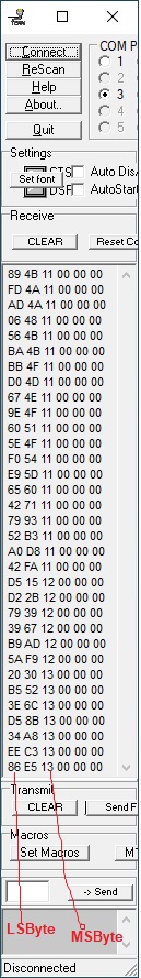
The reason why I think it may not be 62CAD4 is because:
a) I have configured the UART of my uC as LSB first, so as to match the ADC code output format.
b) In my test setup, when I increase the temperature of PT100 (using Hot air Blower)- 
    the MSByte 'D4' remains most stable, 'CA' varies slightly more and LSByte '62' continuously varies.
With rise in temperature there is a drop in this count (and vice versa) i.e.  MSByte changes as D3....D2.....D1.
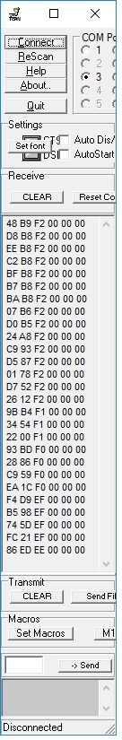
 .....and so on. 
In the image that I have inserted (with Rref = 6.8Kohm), the count is even bigger, and the change can be seen as I described.
Regarding Gain, yes you guessed it right, I have set the Gain as 16.  

Now, Regarding the problem that I am facing with IDAC:
As you know I am using Ratiometric measurement configuration.
I am observing that irrespective of the IDAC value that I select in Configuration Register 2,
the IDAC is getting decided by DVDD (3.3vdc) and Rref (1.65K or 3.3K or 6.8K) that I connect across REFP and REFN.
With Rref=6.8K, the IDAC is 0.483mA (approx 0.5mA)
With Rref=3.3K, the IDAC is 0.96mA (approx 1mA)
With Rref=1.65K,the IDAC is 1.909mA (approx 2mA) and
Thus, I observe different values of IDAC while the one selected by me in Config Reg2 is constant i.e. 500uA.
So, the selection of IDAC value in Config Reg2 seems to have no effect on the actual value of IDAC.
Can you please suggest why this may be happening? Kindly see the inserted image2 below:


Thank you once again,
Best Regards,
Milind Risbud.

  • Hi Milind,

    As I was explaining before the ADS122U04 transmits LSB first which means that the data are in the order of D0, D1, D2, ..., D21, D22, D23.  The micro will shift the bit order for each byte so that D0, D1, D2, D3, D4, D5, D6, D7 for byte 0 (B0) so that the order is reversed to D7, D6, D5, D4, D3, D2, D1, D0, but the actual byte order transmitted will be B0, B1 and B2 and as a value should be stored as B2, B1, and B0.  The micro will not automatically do this for you unless using Little Endian format for memory storage.  So when reading the data you need to store properly in your memory variable and sign-extend appropriately if needed.

    Your reference resistor should be a precision resistor with a low temperature coefficient.  A 0.1% resistor tolerance is usually not good enough.

    Regarding IDAC compliance voltage, you need to make sure that you are not attempting to operate outside of the IDAC compliance range which as per datasheet is AVDD - 0.9V.  This means that the total voltage drop of the current path (RTD and reference resistor) cannot exceed the compliance voltage or the constant current source cannot maintain a constant value.  For 3.3V operation this would be 2.4V.  If the IDAC is set to 500uA and you use the 6.8k value of resistance, 6.8k * 500uA = 3.4 V which exceeds the compliance range as well as the supply voltage.

    How are you actually determining the current?  Are you measuring across the Rref resistor with a voltmeter?  Can you tell me what the voltages are for each resistor?  However 6.8k will never work.  You should see about 1.65V for 3.3k and about 825mV for 1.65k.  You would also need to reduce your gain most likely for the 1.65k Rref.

    Best regards,

    Bob B

  • Hello Bob,
    To determine the current (flowing through the current path), I am measuring the voltage across Rref-
    and dividing it by the value of Rref.
    For e.g.:
    Presently the Rref value is 1.65Kohms (MFR)....later I will be using a  resistor with a low temperature coefficient.
    and the voltage measured across Rref is 3.12Vdc.
    so, IDAC1 = (3.12Vdc/1.65Kohm) 
    so, IDAC1 = 1.890 milliAmperes

    Regarding the voltages across PT100 and Rref (1.65Kohm) :-

    • The voltage measured across Rref is:      3.12Vdc and
    • The voltage measured across PT100 is:  0.211Vdc

    Thus, the sum-total of these above two voltages is 3.33vdc which is equal to DVDD and AVDD.

    You have mentioned that the total voltage drop of the current path should be 2.4vdc when DVDD = AVDD =3.3vdc,
    but what I am observing in this circuit is that, irrespective of the Rref value that I connect, and irrespective of the IDAC1 value that I select-
    the voltage across Rref is always above 3vdc , i.e.:

    With Rref = 3.3Kohm,   the voltage across Rref is 3.20vdc and that across PT100 is 0.10vdc
    With Rref = 1.65Kohm, the voltage across Rref is 3.12vdc and that across PT100 is 0.21vdc
    With Rref = 6.8Kohm,   the voltage across Rref is 3.28vdc and that across PT100 is 0.02vdc

    I don't understand why this is happening and I don't know what should I do to ensure that the total voltage drop of the current path remains 2.4vdc !
     
    Now, regarding the sequence of bits and bytes as they arrive for ADC:-
    I have ensured that UART of my micro is configured for LSB first data reception and-
    the compiler is configured to save data in the memory of micro in 'Little Endian' format.
    So, if we again go back to the example of three byte data 'D4CA62' received, I am receiving it as:

    Byte0: 62
    Byte1: CA
    Byte2: D4

    And I am interpretting it in the reverse order i.e. 'D4CA62' and the fact that, with variation in temperature-
    'D4' is seen to remains most stable and varies after large change in temperature, where as 'CA' varies prior to that and '62' is most volatile.
    This gives me the impression that 'D4' is the MSbyte of received count.
    [You will notice this in the data log that I inserted in my earlier message, in which MSbyte is seen to vary the least i.e. F2.....F1.....F0......EF......EE and so on]

    I have inserted, with this message, a snap of this ADC circuit that I am working on, and that of the entire test setup (micro + ADC).
    Please give your suggestion, regarding both the above points that I have mentioned.

    Thank you,
    Best Regards,
    Milind Risbud.

  • Hi Milind,

    Although I cannot see your entire circuit connection, I believe that you must have something incorrectly connected.  It may have something to do with the yellow wires.

    You should not see a negative input voltage for the RTD measurement.  Note the current path.  Also, the total voltage drop across the RTD and reference resistor should not be adding up to 3.3V.  This would seem to me that you are voltage exciting the RTD instead of using the IDAC for current excitation.  Below is the circuit you described earlier:

    If you are using the current excitation as shown, with 500uA you should measure 825mV for 1.6k Ohm Rref and 1.65V for 3.3k Ohms Rref.  In this circuit you should not be measuring mA of current, and with 500uA you cannot even make a measurement at all.  So I believe that your circuit is not built as shown previously.  This actual response should be as shown in the following diagram:

    The IDAC current is supplied by AVDD and the maximum voltage Vmax, must be limited to a total voltage drop of less than AVDD - 0.9V.  The current source requires some voltage to power the constant current source, which limits the total voltage drop across the RTD and the Rref resistances.  You need to design your circuit such that when using the IDAC current, the total voltage drop of the maximum resistance of the RTD and the Rref times the IDAC current does not exceet Vmax.

    Best regards,

    Bob B

  • Hello Bob,
    In followup with the work I am doing, as informed earlier, I have connected PT100 in ratiometric configuration. Presently there are two problems that I am facing, which are as fllows:
     
    1. The voltage across Rref and PT100 is always seen as zero.
        This means IDAC1 (or IDAC2...whichever is selected) simply does Not flow.
        I do not understand why this should happen.
        The Dvdd=Avdd=3v3 and Reset pin voltage is also 3v3 but pins 8&9 (Ref voltage input) and
        pins10&11(Analog input pins) always show zero volts with reference to ground.
     
    2. I am reading back all the Configuration Register values after writing them (for verification purpose).
        What I observe is that, the value of "Configuration Register 3" is always read back as "0x83", even
        though the value that I write is "0x80". 
        This means that even though I am trying to select "Manual data read mode",
        what actually gets set is "Automatic data read mode". 
        I do not understand why this should happen. It seems less possible that both these problems
        (i.e. point1 and point2) are related because data output mode and IDAC1 or IDAC1 don't seem
        to be related. The interesting thing is that all other Configuration Registers contain exactly those
        values that I have written into them, but this does not happen in case of 
        "Configuration Register 3".  "Configuration Register 3" always reads back as 0x83.
     
    What I tried doing is that, Instead of continuous conversion mode, I tried using single-shot mode, but this didn't help in any way. So looks like it has nothing to do with the problem.
    Then, I assembled one more ADS122U04 test circuit (just in case any problem with one I was testing with), but same problems are observed in this  second test circuit also. Please find as attachment a screencapture showing the 24bit A/D converted data read from the ADS122U04.
    Kindly suggest, what can be the problem?
    Regards,
    Milind Risbud
  • Hi Milind,

    Before writing to any of the registers I would suggest reading from them first and making sure you see the default values.  Then write and read one register at a time to verify.  Do not set automatic mode or continuous conversion mode at this time.

    If you are able to read and write registers correctly, then check to see if current is flowing from the IDAC through your RTD circuit.  Resolve this issue by external voltage measurement before attempting to convert data. Once you have current flowing and the voltages as expected, then in single conversion mode start a conversion and wait for completion, then use the RDATA command and read the results.

    If you still are having issues, send me the configuration register settings you are using.  Also, verify all your connections.  Usually this is a missing ground connection in these prototype situations.

    Best regards,

    Bob B

  • Hello Bob,

    Thank you for your inputs.
    As you suggested, I did the following:-
    a) After Microcontroller powerup [and initialization of UART1 (for communication with    
        ADS122U04) and UART5 (for sending out values to PC for debug purpose)], I just sent out the 
        RESET command to  ADS122U04 and after that allowed a delay (in firmware) of 1 Second.
    b) After this I read the values of Config Reg 0 to Config Reg 4, one-after-another. 
        What is observed is that, other than ' Config Reg 3' all other config Regs contain 
        default (Reset)  values, but  ' Config Reg 3'  value keeps varying (as seen in it's value output  
        on UART5 every 1.5second). As seen in the screencap attached, the  value of ' Config Reg 3'
        is most of the time "0x02" or "0x03". I don't understand why this should happen as the code 
        section in firmware for reading the values of these Regs is exactly identical.     
    The values of Config Reg that I set in actual code (not above test code) are as follows:-
    /*Commands for Writing to the 'Configuration Registers' of ADC ADS122U04 IC*/
    uint8_t CMD_WRITE_CONFIGREG_ZERO_ADC_PT100[3]  = {0x55,0x40,0x35}; //PGA enabled,Gain=16,AIN0 and AIN1 as differential analog inputs
    uint8_t CMD_WRITE_CONFIGREG_ONE_ADC_PT100[3]   = {0x55,0x42,0x0A};//Internal 2.048vdc as ref.,Continuous conv.,Normal mode,Data Rate 20SPS
    uint8_t CMD_WRITE_CONFIGREG_TWO_ADC_PT100[3]   = {0x55,0x44,0x05};//Data counter disabled,IDAC1=500uA,Data integrity check disabled
    uint8_t CMD_WRITE_CONFIGREG_THREE_ADC_PT100[3] = {0x55,0x48,0x80};//Manual data read mode,IDAC2 disabled, IDAC1 connected to AIN3
    uint8_t CMD_WRITE_CONFIGREG_FOUR_ADC_PT100[3]  = {0x55,0x4A,0x00};//GPIO2 configured as input which is default setting
    Attached are the '.c' files containing ADC related functions and main() function for your reference.

    /*---------------------------------------------------------------------------------
    * PT100_SensorRead.c
    *
    * Created on: 19-Jun-2020
    * Author: Milind Risbud
    ---------------------------------------------------------------------------------*/

    //---------------------------------------------------------------------------------
    #include "r_cg_macrodriver.h"

    //---------------------------------------------------------------------------------
    //Note:
    //[1] UART of uC needs to be configured as follows for communication with ADC ADS122U04 IC
    // Data bits=8
    // Parity=NONE
    // Stop Bits=1
    //[2] ADC IC ADS122U04 has a universal asynchronous receiver transmitter (UART)compatible interface-
    // for command and data transfer between the uC and ADS122U04 IC.
    // The interface is half-duplex, meaning only either the uC or the ADS122U04 can communicate at any given time.
    // The ADS122U04 actively synchronizes to the baud rate of the uC using the Synchronization Byte (0x55) that-
    // has to be sent by uC prior to each and every Command. Thus, this 'baud rate Synchronization' happens every time-
    // a command is sent by uC to ADS122U04 IC.
    // Output data from ADS122U04 IC can be register contents or conversion results.
    //[3] Here the ADC IC is configured to work in "CONTINUOUS CONVERSION" mode and-
    // the A/D converted data output mode of the ADC IC is configured to be "MANUAL DATA READ" mode-
    // which is it's default mode (instead of Automatic data read mode).
    //---------------------------------------------------------------------------------
    //Constants Declaration
    #define PT100_ADC_RECBUFFLEN_MAX 6
    #define ADC_CONFIG_READBACK_MAXLEN 10
    //NOTE:- Value "0x55" hex is the "Synchronization Byte" needed to be sent before every command to ADC ADS122U04 IC.
    // That is the reason why this value "0x55" hex is seen as the very first byte of each of the command array.
    //Stand-alone commands (i.e. instructions) to ADC ADS122U04 IC
    uint8_t CMD_RESET_ADC_PT100[2] = {0x55,0x06};
    uint8_t CMD_STARTSYNC_ADC_PT100[2] = {0x55,0x09};
    uint8_t CMD_POWERDOWN_ADC_PT100[2] = {0x55,0x02};
    uint8_t CMD_READDATA_ADC_PT100[2] = {0x55,0x1C};

    //Commands for Reading the 'Configuration Registers' of ADC ADS122U04 IC
    uint8_t CMD_READ_CONFIGREG_ZERO_ADC_PT100[2] = {0x55,0x20};
    uint8_t CMD_READ_CONFIGREG_ONE_ADC_PT100[2] = {0x55,0x22};
    uint8_t CMD_READ_CONFIGREG_TWO_ADC_PT100[2] = {0x55,0x24};
    uint8_t CMD_READ_CONFIGREG_THREE_ADC_PT100[2] = {0x55,0x28};
    uint8_t CMD_READ_CONFIGREG_FOUR_ADC_PT100[2] = {0x55,0x2A};

    //Commands for Writing to the 'Configuration Registers' of ADC ADS122U04 IC
    uint8_t CMD_WRITE_CONFIGREG_ZERO_ADC_PT100[3] = {0x55,0x40,0x35}; //PGA enabled,Gain=16,AIN0 and AIN1 as differential analog inputs
    uint8_t CMD_WRITE_CONFIGREG_ONE_ADC_PT100[3] = {0x55,0x42,0x0A}; //Internal 2.048vdc as ref.,Continuous conv.,Normal mode,Data Rate 20SPS
    uint8_t CMD_WRITE_CONFIGREG_TWO_ADC_PT100[3] = {0x55,0x44,0x05}; //Data counter disabled,IDAC1=500uA,Data integrity check disabled
    uint8_t CMD_WRITE_CONFIGREG_THREE_ADC_PT100[3] = {0x55,0x48,0x80}; //Manual data read mode,IDAC2 disabled, IDAC1 connected to AIN3
    uint8_t CMD_WRITE_CONFIGREG_FOUR_ADC_PT100[3] = {0x55,0x4A,0x00}; //GPIO2 configured as input which is default setting

    //---------------------------------------------------------------------------------
    //Variables Declaration
    uint8_t PT100_ADC_DataReceiveBuff[PT100_ADC_RECBUFFLEN_MAX] = {0x00,0x00,0x00,0x00,0x00,0x00};
    uint8_t PT100_ADC_ConfigRegReadBackBuff[ADC_CONFIG_READBACK_MAXLEN] = {0x00,0x00,0x00,0x00,0x00,0x00,0x00,0x00,0x00,0x00};


    //---------------------------------------------------------------------------------
    //Functions Declarations -These must be done after variable declaration otherwise-
    //IDE misbehaves i.e. compiler says zero errors but bugs symbols seen-
    //(for e.g. in case of 'OperatingMode.c' file), the 'stTime' structure elements-
    //and they are signaled as undefined.
    void InitADCandStartConversion_PT100(void);
    void PT100_ClearADCdatareceivebuffer(void);
    void ReadADC_ConversionResult_PT100(void);
    void ReadBackConfigRegs(void);
    //---------------------------------------------------------------------------------
    //Functions Definitions
    //~~~~~~~~~~~~~~~~~~~~~~~~~~~~~~~~~~~~~~~~~~~~~~~~~~~~~~~~~~~~~~~~~~~~~~~
    //Function Name: InitADCandStartConversion_PT100
    //Description: Initialize the external ADC IC ADS122U04, and Start A/D conversion.
    //Here the ADC IC is configured to work in "CONTINUOUS CONVERSION" mode and-
    //the A/D converted data output mode of the ADC IC is configured to be "MANUAL DATA READ" mode-
    //which is it's default mode (instead of Automatic data read mode).
    //-----------------------------------------------------------------------
    void InitADCandStartConversion_PT100(void)
    {
    //Send the sync byte and RESET command to PT100 ADC
    R_SCI1_Serial_Send(CMD_RESET_ADC_PT100,2);
    delay_1000msec();
    //--------------------------------------------------------------------------
    //Write the respective register configurations with the WREG command, sending the synchronization byte each time
    R_SCI1_Serial_Send(CMD_WRITE_CONFIGREG_ZERO_ADC_PT100,3); //write setting bits to configuration reg0
    delay_100msec();
    delay_100msec();
    delay_50msec();
    R_SCI1_Serial_Send(CMD_WRITE_CONFIGREG_TWO_ADC_PT100,3); //write setting bits to configuration reg2
    delay_100msec();
    delay_100msec();
    delay_50msec();
    R_SCI1_Serial_Send(CMD_WRITE_CONFIGREG_THREE_ADC_PT100,3); //write setting bits to configuration reg3
    //delay_100msec();
    //delay_100msec();
    delay_500msec();
    R_SCI1_Serial_Send(CMD_WRITE_CONFIGREG_FOUR_ADC_PT100,3); //write setting bits to configuration reg4
    delay_100msec();
    delay_100msec();
    delay_50msec();
    //Now, write to the config reg1 so as to select 'Continuous Conversion mode'
    R_SCI1_Serial_Send(CMD_WRITE_CONFIGREG_ONE_ADC_PT100,3); //write setting bits to configuration reg1
    //delay_100msec();
    //delay_100msec();
    delay_50msec();
    //-------------------------------------------------------------------------------
    //Send the START/SYNC command to start converting in continuous conversion mode
    //The START/SYNC command needs to be given immediately after Setting (logic one) the Configuration mode 'CM' bit in-
    //config reg1 which indicates that 'Continuous Conversion mode' is enabled.
    R_SCI1_Serial_Send(CMD_STARTSYNC_ADC_PT100,2);
    delay_500msec();
    }//end of function void InitADCandStartConversion_PT100(void) ends


    //---------------------------------------------------------------------------------
    //Function Name: PT100_ClearADCdatareceivebuffer
    //Description: Clear the PT100 ADC data receive buffer and-
    // re-initialize uart1 serial reception buffer counter
    //-----------------------------------------------------------------------
    void PT100_ClearADCdatareceivebuffer(void)
    {
    uint8_t ucClearLoopCtr;
    for (ucClearLoopCtr=0x00;ucClearLoopCtr<PT100_ADC_RECBUFFLEN_MAX;ucClearLoopCtr++)
    {
    PT100_ADC_DataReceiveBuff[ucClearLoopCtr] = 0x00;
    }//end of for loop
    R_SCI1_Serial_Receive(PT100_ADC_DataReceiveBuff,PT100_ADC_RECBUFFLEN_MAX); //re-initialize uart1 serial reception buffer counter
    }//end of function PT100_ClearADCdatareceivebuffer ends
    //---------------------------------------------------------------------------------
    //Function Name: ReadADC_ConversionResult_PT100
    //Description:
    //-----------------------------------------------------------------------
    void ReadADC_ConversionResult_PT100(void)
    {
    uint8_t ucStatusTemp;

    //Send the START/SYNC command to start converting in Single-shot conversion mode
    //R_SCI1_Serial_Send(CMD_STARTSYNC_ADC_PT100,2);
    //delay_500msec();
    //Clear the PT100 ADC data receive buffer and re-initialize uart1 serial reception buffer counter
    PT100_ClearADCdatareceivebuffer();
    //Send Command to Read the contents of Config Reg2 so as to check the status of "DRDY" (Bit7)-
    //If ("DRDY" bit==1) it means that "New conversion result ready" for the host uC to read.
    R_SCI1_Serial_Send(CMD_READ_CONFIGREG_TWO_ADC_PT100,2);
    delay_100msec();
    delay_100msec();
    delay_50msec();
    //Receive the contents of Config Reg2
    R_SCI1_Serial_Receive(PT100_ADC_DataReceiveBuff,PT100_ADC_RECBUFFLEN_MAX);
    delay_500msec();

    ucStatusTemp = PT100_ADC_DataReceiveBuff[0]; //copy the value of Config Reg2 into temporary var
    if(ucStatusTemp&0xF0) //mask all other bits except data ready status flag 'DRDY' bit7
    {
    //Clear the PT100 ADC data receive buffer and re-initialize uart1 serial reception buffer counter
    PT100_ClearADCdatareceivebuffer();
    //send command to read A/D converted data
    R_SCI1_Serial_Send(CMD_READDATA_ADC_PT100,2);
    delay_100msec();
    delay_100msec();
    delay_50msec();
    //Receive the A/D converted data sent by ADC IC
    R_SCI1_Serial_Receive(PT100_ADC_DataReceiveBuff,PT100_ADC_RECBUFFLEN_MAX);
    delay_1000msec();//delay needed for serial transmission to complete via ISR
    }
    //send the received data on UART5 for monitoring purpose
    R_SCI5_Serial_Send(PT100_ADC_DataReceiveBuff,PT100_ADC_RECBUFFLEN_MAX);
    delay_100msec();
    delay_100msec();
    delay_50msec();
    }//end of function ReadADC_ConversionResult_PT100 ends
    //-----------------------------------------------------------------------


    //-----------------------------------------------------------------------
    //Function Name: ReadBackConfigRegs
    //Description: Read Back the config reg contents to verify that they have got written correctly
    //-----------------------------------------------------------------------
    void ReadBackConfigRegs(void)
    {
    //------------------------------
    //Clear the PT100 ADC data receive buffer and re-initialize uart1 serial reception buffer counter
    PT100_ClearADCdatareceivebuffer();
    //Read Back the config reg contents to verify that they have got written correctly
    R_SCI1_Serial_Send(CMD_READ_CONFIGREG_ZERO_ADC_PT100,2);
    delay_100msec();
    //Receive the contents of Config Reg
    R_SCI1_Serial_Receive(PT100_ADC_DataReceiveBuff,PT100_ADC_RECBUFFLEN_MAX);
    delay_100msec();
    delay_100msec();
    delay_50msec();
    PT100_ADC_ConfigRegReadBackBuff[0] = PT100_ADC_DataReceiveBuff[0];
    //------------------------------
    //Clear the PT100 ADC data receive buffer and re-initialize uart1 serial reception buffer counter
    PT100_ClearADCdatareceivebuffer();
    //Read Back the config reg contents to verify that they have got written correctly
    R_SCI1_Serial_Send(CMD_READ_CONFIGREG_ONE_ADC_PT100,2);
    delay_100msec();
    //Receive the contents of Config Reg
    R_SCI1_Serial_Receive(PT100_ADC_DataReceiveBuff,PT100_ADC_RECBUFFLEN_MAX);
    delay_100msec();
    delay_100msec();
    delay_50msec();
    PT100_ADC_ConfigRegReadBackBuff[1] = PT100_ADC_DataReceiveBuff[0];
    //------------------------------
    //Clear the PT100 ADC data receive buffer and re-initialize uart1 serial reception buffer counter
    PT100_ClearADCdatareceivebuffer();
    //Read Back the config reg contents to verify that they have got written correctly
    R_SCI1_Serial_Send(CMD_READ_CONFIGREG_TWO_ADC_PT100,2);
    delay_100msec();
    //Receive the contents of Config Reg
    R_SCI1_Serial_Receive(PT100_ADC_DataReceiveBuff,PT100_ADC_RECBUFFLEN_MAX);
    delay_100msec();
    delay_100msec();
    delay_50msec();
    PT100_ADC_ConfigRegReadBackBuff[2] = PT100_ADC_DataReceiveBuff[0];
    //------------------------------
    //Clear the PT100 ADC data receive buffer and re-initialize uart1 serial reception buffer counter
    PT100_ClearADCdatareceivebuffer();
    //Read Back the config reg contents to verify that they have got written correctly
    R_SCI1_Serial_Send(CMD_READ_CONFIGREG_THREE_ADC_PT100,2);
    delay_100msec();
    //Receive the contents of Config Reg
    R_SCI1_Serial_Receive(PT100_ADC_DataReceiveBuff,PT100_ADC_RECBUFFLEN_MAX);
    delay_100msec();
    delay_100msec();
    delay_50msec();
    PT100_ADC_ConfigRegReadBackBuff[3] = PT100_ADC_DataReceiveBuff[0];
    //------------------------------
    //Clear the PT100 ADC data receive buffer and re-initialize uart1 serial reception buffer counter
    PT100_ClearADCdatareceivebuffer();
    //Read Back the config reg contents to verify that they have got written correctly
    R_SCI1_Serial_Send(CMD_READ_CONFIGREG_FOUR_ADC_PT100,2);
    delay_100msec();
    //Receive the contents of Config Reg
    R_SCI1_Serial_Receive(PT100_ADC_DataReceiveBuff,PT100_ADC_RECBUFFLEN_MAX);
    delay_100msec();
    delay_100msec();
    delay_50msec();
    PT100_ADC_ConfigRegReadBackBuff[4] = PT100_ADC_DataReceiveBuff[0];
    //------------------------------
    //send the received data on UART5 for monitoring purpose
    R_SCI5_Serial_Send(PT100_ADC_ConfigRegReadBackBuff,PT100_ADC_RECBUFFLEN_MAX);
    delay_100msec();
    delay_100msec();
    delay_50msec();
    }
    //-----------------------------------------------------------------------END OF FILE PT100_SensorRead.c-----------------------------------------------------------

    //-----------------------------------------------------------------------START OF FILE main.c-----------------------------------------------------------

    /***********************************************************************************************************************
    * File Name : r_cg_main.c
    * Version : Code Generator for RX113 V1.02.05.01 [11 Nov 2016]
    * Device(s) : R5F51136AxFM
    * Tool-Chain : CCRX
    * Description : This file implements main function.
    * Creation Date: 21-Jun-20
    ***********************************************************************************************************************/

    /***********************************************************************************************************************
    Pragma directive
    ***********************************************************************************************************************/
    /* Start user code for pragma. Do not edit comment generated here */
    /* End user code. Do not edit comment generated here */

    /***********************************************************************************************************************
    Includes
    ***********************************************************************************************************************/
    #include "r_cg_macrodriver.h"
    #include "r_cg_cgc.h"
    #include "r_cg_port.h"
    #include "r_cg_rtc.h"
    #include "r_cg_iwdt.h"
    #include "r_cg_sci.h"
    #include "r_cg_riic.h"
    /* Start user code for include. Do not edit comment generated here */
    #include "stdint.h"
    #include "CommonDefines.h"
    /* End user code. Do not edit comment generated here */
    #include "r_cg_userdefine.h"

    /***********************************************************************************************************************
    Global variables and functions
    ***********************************************************************************************************************/
    /* Start user code for global. Do not edit comment generated here */

    //------------------------------------------------------------------------------------
    uint8_t ucTestToggle = 0x00; // for test purpose only

    rtc_calendarcounter_value_t GSM_nw_Time; // get the GSM network time in his structure
    uint8_t Hours,Minutes,Seconds;
    uint8_t Year,Month,Day;
    uint8_t Temp_Var;
    uint8_t Year_Decimal,Month_Decimal,Day_Decimal;
    uint8_t Hours_Decimal,Minutes_Decimal,Seconds_Decimal;
    extern volatile uint8_t Send_End;

    //typedef struct
    //{
    // uint8_t ucSecond;
    // uint8_t ucMinute;
    // uint8_t ucHour;
    // uint8_t ucDay;
    // uint8_t ucWeek;
    // uint8_t ucMonth;
    // uint16_t uiYear;
    //} DateAndTime_t;
    //DateAndTime_t stDMYHMS_BCD,stDMYHMS_Decimal;

    //structures used when updating latest GSM date and time periodically
    rtc_calendarcounter_value_t stDateTimeBCD,stDateTimeDecimal;

    rtc_calendar_alarm_enable_t stAlarmEnable;
    rtc_calendar_alarm_value_t stAlarmTime;

    //An unsigned long value used as input parameter to srand() function that-
    //sets an initial value of the pseudo-random number sequence generated by the rand() function.
    //Functions srand() and rand() are used for generating the 'Main Interval' of random duration-
    //in minutes (20min to 60min) when 'Main Interval Type' is set as 'RANDOM' via Settings SMS.
    uint32_t ulSeedValueForRandomNumFunct = 0x00000000; // A 32bit initialization value


    uint8_t LineFeed[1] ={0x0A};
    uint8_t cmd1[] ={"AT\r"};
    uint8_t cmd2[] ={"ATD"};
    uint8_t PhoneNum[] ={"9423570299;"};
    uint8_t cmd3[] ={"ATH"};
    uint8_t cmd4[] ={"AT+CMGF=1\r"}; //select TEXT mode
    uint8_t cmd6[] ={"AT+QINISTAT\r"};
    uint8_t cmd7[] ={"AT+QNSTATUS\r"};
    uint8_t cmd8[] ={"AT+QNITZ=0\r"};//After receiving network time message, DO-NOT send URC (unsolicited Result)
    uint8_t cmd9[] ={"AT+CCLK?\r"};
    uint8_t cmd10[] ={"ATE0\r"};
    uint8_t cmd11[] ={"AT+CMGD=1,4\r"}; //Delete SMS,ALL
    uint8_t cmd13[] ={"AT+CTZU=3\r"}; //Network Time Synchronization and Update the RTC Time
    uint8_t cmd14[] ={"AT+CSCS="}; //send command AT+CSCS="IRA" to set the character set to IRA
    uint8_t cmd15[] ={"AT+CSCS?\r"};
    uint8_t chset_IRA[] ={"IRA"};
    uint8_t chset_HEX[] ={"HEX"};
    uint8_t chset_GSM[] ={"GSM"};
    uint8_t DoubleQuote[1] ={0x22}; //double-quote character hex code
    uint8_t Comma_Char[1] ={0x2c}; //Comma character hex code
    uint8_t cmd16[] ={"AT+QMGDA=6\r"}; //Delete all SMS - PDU MODE
    uint8_t cmd17[] ={"AT+CMGF=0\r"}; //select PDU mode
    uint8_t cmd18[] ={"AT+QMGDA="}; //Delete all SMS
    uint8_t DEL_ALL[] ={"DEL ALL"}; //string send as parameter following "AT+QMGDA=" command to delete all SMS
    uint8_t DummySMS[] = {"Hello Evincere"};
    uint8_t cmd19[] ={"AT&W\r"}; // command for Storing the current settings in M66 user profile
    uint8_t cmd20[] ={"AT+CPMS="}; // Set the SMS storage memory as SIM memory
    uint8_t SIM_mem[] ={"SM"}; //used when sending the command:AT+CPMS="SM","SM","SM";here SM means SIM memory
    uint8_t cmd21[] ={"AT+CREG?\r"}; //Get network registration status of M66 module
    //_Bool TestVar;
    //------------------------------------------------------------------
    //Function Declarations
    //------------------------------------------------------------------
    void delay_625msec(void); // for 5sec delay
    void delay_6msec(void); // for 50msec delay
    void delay_50msec(void); // for 50msec delay
    void delay_500msec(void); // for 500msec delay
    void delay_100msec(void); // for 100msec delay
    void delay_1000msec(void);// for 1000msec delay
    void ClearReceiveBuffer(void);
    void UpdtNwTimeToRTC(void);
    void SetAlarmTime(uint8_t);
    void Disable_RTCAlarm(void);
    void SetUnitPowerupSMSFlags(void);
    void ObtainGSMtimeInRuntime(void);
    //------------------------------------------------------------------
    /* End user code. Do not edit comment generated here */


    static void R_MAIN_UserInit(void);
    /***********************************************************************************************************************
    * Function Name: main
    * Description : This function implements main function.
    * Arguments : None
    * Return Value : None
    ***********************************************************************************************************************/
    void main(void)
    {
    R_MAIN_UserInit();
    /* Start user code. Do not edit comment generated here */
    PORT2.PODR.BIT.B7=0; //ACK LED OFF
    PORT2.PODR.BIT.B6=0; //BUZZER OFF
    delay_100msec();
    while (1U)
    {
    //----------------------------------
    PORT2.PODR.BIT.B7=1; //ACK LED ON
    PORT2.PODR.BIT.B6=1; //BUZZER ON
    delay_500msec();
    PORT2.PODR.BIT.B7=0; //ACK LED OFF
    PORT2.PODR.BIT.B6=0; //BUZZER OFF
    delay_500msec();
    //----------------------------------
    //----------------------------------
    ReadADC_ConversionResult_PT100();
    //Send the sync byte and RESET command to PT100 ADC
    //ReadBackConfigRegs();
    }
    //-----------------------------------------------------------------------------
    /* End user code. Do not edit comment generated here */
    }
    /***********************************************************************************************************************
    * Function Name: R_MAIN_UserInit
    * Description : This function adds user code before implementing main function.
    * Arguments : None
    * Return Value : None
    ***********************************************************************************************************************/
    void R_MAIN_UserInit(void)
    {
    /* Start user code. Do not edit comment generated here */
    delay_500msec();
    R_SCI1_Start(); //initialization of UART1
    nop();nop();nop();nop();nop();nop();nop();nop();nop();nop();
    R_SCI5_Start(); //initialization of UART5
    nop();nop();nop();nop();nop();nop();nop();nop();nop();nop();
    InitADCandStartConversion_PT100(); //initialization of ADS122U04
    nop();nop();nop();nop();nop();nop();nop();nop();nop();nop();
    /* End user code. Do not edit comment generated here */
    }

    /* Start user code for adding. Do not edit comment generated here */
    //-----------------------------------------------------------------------
    /***********************************************************************************************************************
    * Function Name: delay
    * Description : This function clears the receive buffer
    * Arguments : None
    * Return Value : None
    ***********************************************************************************************************************/
    void ClearReceiveBuffer(void)
    {
    uint16_t i;
    for(i=0;i<SMS_RECBUFFLEN_MAX;i++)
    {
    ReceiveBuffer[i] = 0x00; // clear the receive buffer
    }
    R_SCI9_Serial_Receive(ReceiveBuffer,SMS_RECBUFFLEN_MAX); //re-initialize uart0 serial reception buffer counter
    }

    /***********************************************************************************************************************
    * Function Name: delay_50msec
    * Description : This function implements a delay of 50msec at 16MHz Main clk.
    * Measured using Frequency Gen/Counter and verified that 50msec delay is obtained.
    * Arguments : None
    * Return Value : None
    ***********************************************************************************************************************/
    void delay_50msec(void)
    {
    uint16_t outerloop,innerloop;
    for(outerloop=0;outerloop<100;outerloop++)
    {
    for(innerloop=0;innerloop<1000;innerloop++)
    {
    continue;
    }
    }
    }
    /***********************************************************************************************************************
    * Function Name: delay_100msec
    * Description : This function implements a delay of 100msec at 16MHz Main clk.
    * Measured using Frequency Gen/Counter and verified that 100msec delay is obtained.
    * Arguments : None
    * Return Value : None
    ***********************************************************************************************************************/
    void delay_100msec(void)
    {
    uint16_t outerloop,innerloop;
    for(outerloop=0;outerloop<200;outerloop++)
    {
    for(innerloop=0;innerloop<1000;innerloop++)
    {
    continue;
    }
    }
    }
    /***********************************************************************************************************************
    * Function Name: delay_500msec
    * Description : This function implements a delay of 500msec at 16MHz Main clk.
    * Yet to be Measured using Frequency Gen/Counter and verified that 500msec delay is obtained.
    * Arguments : None
    * Return Value : None
    ***********************************************************************************************************************/
    void delay_500msec(void)
    {
    uint16_t outerloop,innerloop;
    R_IWDT_Restart(); //Refresh the I-WDT to avoid I-WDT-Reset
    for(outerloop=0;outerloop<1000;outerloop++)
    {
    for(innerloop=0;innerloop<1000;innerloop++)
    {
    continue;
    }
    }
    }
    /***********************************************************************************************************************
    * Function Name: delay_1000msec
    * Description : This function implements a delay of 1000msec at 16MHz Main clk.
    * Yet to be Measured using Frequency Gen/Counter and verified that 1000msec delay is obtained.
    * Arguments : None
    * Return Value : None
    ***********************************************************************************************************************/
    void delay_1000msec(void)
    {
    uint16_t outerloop,innerloop;
    R_IWDT_Restart(); //Refresh the I-WDT to avoid I-WDT-Reset
    for(outerloop=0;outerloop<2000;outerloop++)
    {
    for(innerloop=0;innerloop<1000;innerloop++)
    {
    continue;
    }
    }
    }
    //-----------------------------------------------------------------------
    /* End user code. Do not edit comment generated here */

    //-----------------------------------------------------------------------END OF FILE main.c-----------------------------------------------------------

  • Hi Milind,

    Make sure you are using the correct addressing in your RREG and WREG commands.  Here is an example of what you are writing as RREG:

    //Commands for Reading the 'Configuration Registers' of ADC ADS122U04 IC
    uint8_t CMD_READ_CONFIGREG_ZERO_ADC_PT100[2] = {0x55,0x20};
    uint8_t CMD_READ_CONFIGREG_ONE_ADC_PT100[2] = {0x55,0x22};
    uint8_t CMD_READ_CONFIGREG_TWO_ADC_PT100[2] = {0x55,0x24};
    uint8_t CMD_READ_CONFIGREG_THREE_ADC_PT100[2] = {0x55,0x28};
    uint8_t CMD_READ_CONFIGREG_FOUR_ADC_PT100[2] = {0x55,0x2A};

    However this is only correct for register 0, 1 and 2.  The addressing is bits 3 through 1 of the command, and bit 0 is a 'don't care'.  For ease of discussion I have made bit 0 equal to '0'.

    0000 .-> register 0 and for RREG command would be 0x20 and WREG would be 0x40

    0010 .-> register 1 and for RREG command would be 0x22 and WREG would be 0x42

    0100 .-> register 2 and for RREG command would be 0x24 and WREG would be 0x44

    0110 .-> register 3 and for RREG command would be 0x26 and WREG would be 0x46

    1000 .-> register 4 and for RREG command would be 0x28 and WREG would be 0x48

    So you are incorrectly addressing register 4 and reading/writing register 4 instead of register 3.

    Best regards,

    Bob B

  • Hello Bob,

    Bob, you are Great!
    you exactly pointed out the mistake that I had made.
    I just made that one correction and everything started to work like magic!
    The only thing that I am unable to understand now is that, via Config Reg2,
    I have selected the IDAC value as 500uA, but the actual voltage reading that-
    I am observing across Rref is as if 250uA current is flowing. Details of testing are  as follows:-

    Corrections done:
    For config reg3, read command should be 0x26 and write command should be 0x46. - DONE
    For config reg4, read command should be 0x28 and write command should be 0x48. - DONE

    With above two corrections done, I started getting the 24bit ADC converted count with "MSbit as zero" (and not one)-
    which means it is a positive value (earlier I was getting MSByte as 0xFF)
    Using hot air blower, increased the temperature of PT100 and observed that there is corresponding gradual INCREASE in the 24bit ADC converted value.
    Then, stopped the hot air blower, and observed that there is gradual DECREASE in the 24bit ADC converted value. [Please refer to the attached log file below]

    With Rref = 3.3kOhms and IDAC1 selected as 500uAmps:

    At an ambient (room temp.) of 28 degC,
    The voltage across Rref hovers close to 306mVolts and voltage across PT100 is a steady value of 8mVolts (count = 11 xx xx). 
    With increased temp. of PT100 (using  hot air blower and correspondingly increased count = 16 xx xx) ,
    The voltage across Rref hovers close to 330mVolts 
    and voltage across PT100 is a steady value of 13mVolts.

    My question is that, Rref (3.3k) x IDAC1 (0.5mAmp) should give 1.65Volts across Rref, or something close to this value,
    but I am observing values as if  Rref (3.3k) x IDAC1 (0.25mAmp) i.e. values closer to 825mVolts, which is evident in my readings mentioned above.
    I have re-verified that I have selected  IDAC1 as 500uAmps

    uint8_t CMD_WRITE_CONFIGREG_TWO_ADC_PT100[3]   = {0x55,0x44,0x05}; //Data counter disabled,IDAC1=500uA,Data integrity check disabled

    Can you suggest why this may be happening?

    Regards,

    Milind.


  • Hi Milind,

    Yes, you should see 1.65V across the reference resistor if the current is 500uA and the resistor is 3.3k.  I'm not quite sure what to tell you other than you will need to verify that your total voltage drop from AIN3 to AGND does not the IDAC compliance that I discussed earlier in this thread.  So first verify by register read that the settings are correct, then measure the voltage from AIN3 to AGND and tell me the result.

    Best regards,

    Bob B